|
rf90953a.exe Reference Disk Type 3 Processor Complex v1.11 (zipped image)
rd9095a.exe Diagnostic Disk Type 1 - 4 Processor Complex v2.33 (zipped image)
192-101 IBM PS/2 Enhanced 486/50 Processor Upgrade
Upgrading the Type 3 Complex
Specifications
Memory
Features
"M" / Enhanced 486DX 50 MHz
Base Board
Daughtercard
Daughtercard Rework
Diagnostic LEDs
Block Diagram
Enhanced Memory Parts
Why Double Deck?
Incompatibility with Network Streamers
System Firmware
ROM Images
Support for >1 GB Disks as IML Drive
BIOS ROM Burning
Unsuccessful 50 MHz Processor Installation (H097075)
False ARTIC Diag Error
5x86 Interposer
Specifications
Memory
RAM
- 1 and 2 MB 85 ns parity SIMMs
- 2, 4 and 8 MB 70/80 ns parity SIMMs
- 4 and 8 MB 70 ns ECC SIMMs
- The memory SIMMs must be installed in matched pairs (speed, size and type).
- Mixing Parity and ECC is not allowed, not even if the pairs are matched.
Cache
- L1: 8 KB (486DX)
- L2: 256 KB write-through (standard)
Features
Note: The M complex has the functional
equivalence of the SynchroStream Controller,
but in discrete chips and it doesn't operate quite as fast as the single-chip
solution.
"M" / Enhanced 486DX 50 MHz 82G2484 or 57F1597, FCC ID ANOIBM486B50
![[P]](/other/img/photo.gif "Front")
Base Board sticker 71G6207 or 61G9343
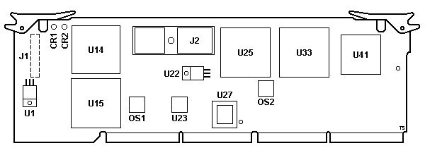
CR1,2 Diagnostic LEDs
J1 Pads for 25-pin header
J2 Daughtercard Connector
OS1 40.0000 MHz osc (Local Bus)
OS2 22.1184 MHz osc (?)
U1 LT1085CT Reg. (2.9 V for U15)
U14 96F1920 Memory Data Buffer
|
U15 96F1921 Memory Address Driver
U22 LT1085CT Reg. (3.7 V for U25 & U33)
U23 87X0079 Clock Generator
U25 10G7459(ESD)
U33 92F1477(ESD)
U27 BIOS ROM (41G9251 '92, 52G9619 '93)
U41 10G7808 DMA Controller (Type 2)
|
U25,33 Memory controller & Bus
Interface Unit (MCA BIU). It's currently unknown which is which.
U27 BIOS ROM Mitsubishi 27C201 (256Kx8)
J1 Unpopulated 2x13 header with one pin
missing. Possibly an earlier implementation of the SDL interface? (the T3 POST
outputs early diag. codes but in different format compared to the T4 platform)
Might include JTAG as well.
J2 Connector between Base and Daughter
cards. 10x11 pins on left, 10x13 pins on right, 240 total.
Base Board Back
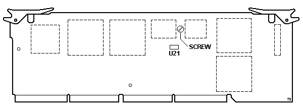
U21 LM339 Voltage comparator
To remove the daughtercard you have to first loosen the
SCREW on the back side of the high speed
connector J2 (see above). Then unlatch the
standoff 1 from the front side of the
daughtercard (see below). You may also have to push through the other smaller
standoff 2. With all this done you should
be able to separate the two boards without any trouble.
Daughtercard sticker 71G6190
OS1 50 MHz osc (CPU)
SP1 Empty or PAL
U1 87X0079 Clock Generator
U2 78F1639 Memory Address Buffer
U3 168-pin LIF CPU socket (486DX-50)
|
U4,5,7-12 TC55B329J-12 32Kx9 SRAM (L2)
U6 96F1992 Memory Data Buffer
U13 92F1379 L2 Cache Controller Set
U18 10G7426 L2 Cache Controller Set
U14,15,17 SN74BCT2160-12FM 8Kx4 TAG RAM
|
SP1 Empty or 71G6205 (mine says 71G6206) PAL accompanied by a PCB rework
Daughtercard Back
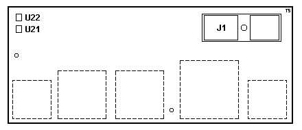
J1 Base Board connector
U21 LM393M Voltage comparator
U22 LM385BM1.2 Voltage ref. diode (1.2 V)
Daughtercard Rework
I have seen one card with the older BIOS 41G9251 ('92) that has NO rework.
The three DX50 I have with the new BIOS 52G9619 ('93) all have the rework.
Why? Haven't a clue.
Ed. The bodge wires are associated with the
additional PAL that was added to the SP1 position on some boards. It connects
the array to the rest of the logic.
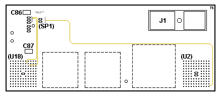
(Click on picture to enlarge)
Diagnostic LEDs
The 50 MHz Type 3 complex in a 90/95, has two LEDs; CR1 and CR2. During
POST, CR1 comes on momentarily and CR2 stays off. If the LEDs work any other
way, suspect that the processor board is defective.
Use the LEDs to help differentiate between a processor board or a system
board failure. If you are instructed to replace one of the boards, and the
problem still exists, replace the other board (also reinstall the first board).
(Ed. Reports coming in make me wonder about any of
this. If the board passes diagnostics, and works normally, do you really care
about the LEDs?)
Block Diagram
A greatly simplified block diagram of the "M" complex:
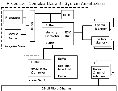
A more detailed version can be found in the following patents:
US5381538,
US5644729,
and US5761533.
Enhanced Memory Parts
Enhanced dual path memory design (Dual Bus Interleave). Although Base 1
allows both the processor and busmasters to access memory concurrently through
two paths, the Base 3 and 4 has buffers at both paths to provide better
performance. Also the buffer on the adapter side (I/O buffer) uses packet data
transfers for writes. This means 16 bytes are collected and this packet is
written in one cycle to memory as opposed to writing for every 4 bytes received
(as with unbuffered systems).
Why Double Deck?
The "M" is the only "double-decker" complex (if we don't count the Type 1
L2 cache daughtercards).
With this complex IBM introduced a set of new features, so the architecture
was quite complex compared to the earlier processor board designs. With the
technological processes used it clearly wasn't possible to fit all the required
logic to a single board. IBM therefore split the design in half, used the base
board for the interface, memory and DMA logic, and moved the CPU subsystem to
a daughtercard.
Incompatibility with Network Streamers
The downlevel processor card FRU 57F1597 is identified by the
lack of a module in position SP1. This card may cause data loss or undetected
change in the:
The upgraded FRU with SP1 is FRU 82G2484 and should be used with these cards.
System Firmware (POST & BIOS)
Simplified firmware stored in EPROM. IML image required for the system to operate.
ROM Images
41G9251 - Unknown
52G9619 - 18 Mar 1992, rev. 0, Mitsubishi M5M27C201 or compat. (position U27, PLCC-32) *
* the same 128K image stored twice or chip incorrectly identified
Support for >1 GB Disks as IML Drive
The M complex supports >1GB drives as the IML source. No complex BIOS
upgrade is needed (or available). However, the SCSI controller needs the
enhanced SCSI BIOS of 92F2244 / 92F2245 to IML properly.
More information HERE.
BIOS ROM Burning
Rick Ekblaw plays deep safety:
The M5M27C201JK is a 2 Megabit part, organized as 256K x 8, with a
12V programming voltage. Logically, it's equivalent to other 2 Megabit EPROMs
in the 27-class, such as the Intel/TI/AMD/Atmel 27C020 or the
Fujitsu/NEC/SGS/ST 27C2001
(see HERE, for example).
However, the DIP form factor was still in common use in this time frame, and
some of the PLCC varieties did not offer a windowed part (One-Time Programming
only).
So, the good news is that you could use almost any 2Mb PLCC32 EPROM or PROM
that you can find to act as a replacement for the M5M27C201JK as the BIOS chip
in your M complex (where it is only being read by the system). For programming
the EPROM/PROM, you have to choose a part for which you have appropriate
algorithms in your programmer, because they vary.
Unsuccessful 50 MHz Processor Installation (H097075)
Interesting challenge on VCF, the OP was unable to boot with an M on a
single serial / single parallel planar. I personally have never had such an
issue, but for the love of God...
Display showed CP80, and I9990021, I9990011 the IML codes were related to
the wrong IML on the SCSI HD and the wrong refdisk... OP had the correct
refdisk, the HD was an 0662-S12 [1,004MB, below 1,024MB], three can Spock
[44/45 SCSI BIOS], and of course, the M [comes stock with enhanced complex
BIOS]. System complaining about the wrong IML code...
"AH-HA! IT LIVES AT LAST! Swapping the position of jumper J16 solved the
issue and got it to finally read from the RefDisk! It only took close to
eighteen months to reach this point but man, does it feel good. Thanks for your
help with this last hiccup, I never would have guessed I'd need to swap a
jumper after installing an M complex."
The RETAIN tip says:
The installation instructions for the 50 MHz processor board, FRU
P/N 92F0048, used in the 8590 and 8595 are incomplete.
Remove the existing complex, then move the override jumper, [8590 - J10,
8595 - J16], so that it connects the center pin and the pin on the opposite end
of the connector. Leave the jumper in this position. [It does not matter if you
change the complex before or after moving the jumper].
Note: The system detects any change in the
Override Jumper position from the last power on, and if it detects a change, it
FORCES it to read the Ref Disk on the next boot -ONLY-. It is a one-shot
wonder.
The system will detect this change and read the Initial Machine Load (IML)
image from the new reference diskette.
False ARTIC Diag Error
Symptom: When running diagnostics on the ARTIC Portmaster Adapter/A
in an 8590 or 8595 with the 486/50MHz processor card installed, a false 14220,
E0DE error may occur.
Problem Isolation Aids: Check the date of the Portmaster Adapter/A
diagnostic file (DEV141.DGS) on the system reference diskette. Files dated
1-31-90 or earlier will exhibit the symptom.
Fix: Download updated
Portmaster Adapter/A
option diskette (self-extracting exe,
zipped image).
5x86 Interposer
I was all set to install a Trinity PowerStacker 5x86 133 MHz on my DX 50 in
the 9595-OMT. I for some reason decided to RTFM while having a cuppa. They say
the PowerStacker will not work with DX 50. What CPU can I use to juice up the
DX 50?
Jim Shorney:
Pay no attention to the manual. Set the multiplier to x3, the
cache jumper (if present) to write-through, and plug it in. It will probably
work fine.
| 