|
rf90954a.exe Reference Disk Type 4 Processor Complex v1.34 (zipped image)
rd9095a.exe Diagnostic Disk Type 1 - 4 Processor Complex v2.33 (zipped image)
Pictorial of failed Type 4 P60/P66 upgrades (by Tam Pham)
"P" & "Q" / Upgrade Pentium 60 MHz & 66 MHz
Old "P" & "Q" Complex Front
Old "P" & "Q" Complex Back
New "Q" Complex Front
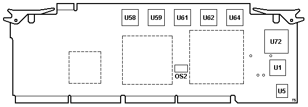
New "Q" Complex Back
Layout Differences
Memory supported, cache
Complex with no CPU and/or L2 Cache Controller
496 vs. 497 Cache Controller
Intel Pentium Overdrive 133 MHz (POD133/120)
Possible Q Upgrade Success!
"P" / Upgrade Pentium 60 MHz FRU P/N 52G9362 or 06H7324, FCC ID ANOIBM586A60
"Q" / Upgrade Pentium 66 MHz FRU P/N 92F0120 or 06H7317, FCC ID ANOIBM586A66
52G9362 and 92F0120 have an early Pentium with the FDIV bug.
06H7324 and 06H7317 come with a fixed processor.
Two slightly different PCB layouts exist.
Old "P" & "Q" Complex Front
P/N 71G6196 ("P")
![[P]](/other/img/photo.gif "P Front") / 06H3817 ("P")
/ 71G6197 ("Q")
PCB P/N 52G9430
/ 06H3817 ("P")
/ 71G6197 ("Q")
PCB P/N 52G9430
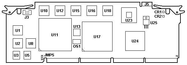
U23 10G3441 - C5C/C8C to SSC BIU (MBC). May
be yellow or blue with exposed die or with a ceramic heat spreader. Peter has
seen a metal capped one. No known issues with any variant.
U25 LT1085CT
Adjustable Voltage Regulator with max. output current 3.0 A. The regulator is
set to 3.7 (3.75) V and powers the SynchroStream Controller.
Old "P" & "Q" Complex Back P/N 71G6196 ("P")
/ 71G6197 ("Q")
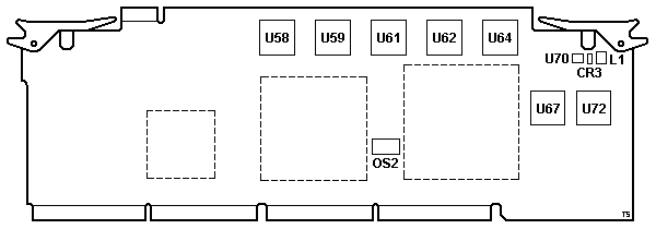
U70, CR3, L1
(plus some other passives) are part of a local 12 V voltage generator.
This additional "programming voltage" (Vpp) is required by the Flash memory
to perform erase/write operations. Its general topology closely replicates
the "Flash Memory VPP Generator" circuit from the
LT1109 datasheet (page 1).
A local 12 V generator is necessary because the processor complex is supplied
with 5 V only.
New "Q" Complex Front P/N 8131364
PCB P/N 71G0226
92F0120 has an early Pentium with the FDIV bug. 06H7317 comes with a fixed processor.
Revised layout similar to the later "Y" complex.
It's possible that this layout was used for some later 60 MHz "P" boards as
well, but this has to be yet confirmed.
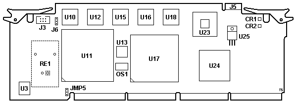
RE1 A provision for a CPU Voltage
Regulator Module (VRM). Pin 1 is marked by a square (bottom-right). Going
clockwise from pin 1, we get: VRM voltage in (+5 V), Ground, Ground, VRM
voltage out (to the CPU). The VRM is not populated on any of the production
boards (at least to our knowledge). Instead, the voltage in and out pins are
shunted by a set of 0 Ω resistors (R210 - R221). In this configuration,
the CPU receives straight 5 V from the PSU - as one would expect from a Socket
4 platform.
Ed. Tom: Why would a P60/66 complex
need a VRM module? I can offer two possible explanations. Some 60/66 MHz
Pentium chips expect a slightly higher supply voltage
(5.15 - 5.40 V),
so the optional VRM may have been added to meet that requirement. It's also
possible that the board was designed for an early iteration of the P54C design
- chips that already used a lower (3.3 or 3.45 V) supply voltage but still came
in the old "Socket 4" PGA package. Know more?
Let Us Know!
New "Q" Complex Back P/N 8131364
Layout Differences
To make room for the VRM component
(RE1) component the area right of the CPU
had to be redesigned. Specifically, a few parts were moved between the
component and solder side and the "new" PCB uses a larger MACH220 PLD to
incorporate logic previously implemented using multiple smaller MACH210
PLDs.
Some other minor changes can be observed too. For example, the
C39 tantalum cap was moved from the back
side of the low-dropout regulator U25 to
the component side to make space for an alternative heatsink mounting/solder
point.
Otherwise, the two board revisions are largely identical. The revised PCB
layout served as the basis for the Type 4 "Y"
board.
Memory
RAM:
PS/2 72-pin SIMMs, ECC or Parity, 70 ns Presence Detect
Min/Max on system board: 8/64 MB Parity, 8/256 MB ECC
ROM:
256 KB (2 x 128 KB) Flash ROM
Cache:
L1: 16 KB (Pentium 60/66)
L2: 256 KB write-back
Complex with no CPU and/or L2 Cache Controller
"P" Complex
Look for a non-FDIV P60 HERE.
S-Spec numbers for 60 MHz Pentium CPUs affected by FDIV-Bug:
P5-60 [A80501-60]: Q0352, Q0394, Q0400, Q0412, Q0466, SX753, SX835, SZ949
A A80501-66 will work just fine.
Look for an A82496-60 Cache controller. An A82496-66 works just as well...
"Q" Complex
Look for a non-FDIV P66 HERE.
S-Spec numbers for 66MHz Pentium CPUs affected by FDIV-Bug:
P5-66 [A80501-66]: Q0353, Q0395, Q0413, Q0467, SX754, SX837, SZ950
Look for an A82496-66 Cache controller. An A82496-60 may or may not work at 66 MHz.
496 vs. 497 Cache Controller
From Dr. Jim Shorney:
Overdrive processors are not compatible with the '496 cache
controller on the P60/66 complexes. However... I swapped out the '496 cache
controller on mine for a borrowed '497 (well heatsinked) and was able to boot
DOS with a POD 133 on my P60 (overclocked to 66). It wasn't entirely stable,
and would not boot OS/2 Warp 4.0 or NT 4.0. The PowerLeap PL54C interposer was
still dead in this configuration. There may yet be hope, I haven't tried the
PowerLeap with anything other than an Intel 166 yet, and I may also downclock
the complex back to 60 MHz and see what happens. There may yet be hope...
The '497 has some 3.3 V supply pins, but it seemed to run stable and
reliable for several hours with the stock P60 CPU in my system in place of the
5 V-only '496. I briefly looked over the docs this afternoon (712 pages,
wow...). Seems the '497 is still a 5 V part, it is the I/O buffers that connect
to the CPU that are 3.3 V. This probably explains in part why the chip doesn't
self-destruct in the '496 socket. It also seems to invalidate the need for an
interposer, since the P60/66 I/O is 5 V anyway and the buffers would have to
run at 5 V to interface at all with the CPU. This brings up the question of
noise immunity, though - will circuits designed to run at 3.3 V logic levels be
more or less sensitive to noise or poor signal quality when run at 5 V?
Inquiring minds want to know.
From Tony Ingenoso:
I suspect noise is going to be less of a problem at higher
voltages Jim. In theory, the voltage range for correct operation would be wider
(particularly for CMOS). The only reason I ever saw (other than laptop
applications) for the drive to lower voltages was to limit heat as the gate
counts and frequencies went up. CMOS parts like high voltages -- you can crank
clock speeds faster with higher voltages(the standard overclockers trick).
Discrete type CMOS parts can often be run as high as 20 V and work fine. The
downside is that its power characteristics start approaching those of TTL at
the higher speeds (and heat goes up). If the only nominally 3.3 V sections of
the cache controller are the line drivers/buffers, there's probably not going
to be enough stuff getting overvoltaged to make any significant difference in
the power draw.
Intel Pentium Overdrive 133 MHz (POD133/120)
From Al Savage:
> So, CPU gurus, will this work in my 8590-OLF w/Type 4 P60?
From Jim Shorney:
You need to stop skipping the meetings, Al... I just tried
this last week, both with and without an Intel EUCD35 interposer. Didn't
work. Sometimes would get as far as CP:8, sometimes wouldn't even post.
I friend of mine here in Lincoln who doesn't read the NG has also tried
it, and he had even less luck then me; his machine wouldn't post at all.
I'm hanging onto my chip, though, in case Tony or someone else
comes up with a solution. I suspect timing loops in the BIOS, but I'm neither
a programmer nor an engineer...
Cache Controller/CPU Incompatibility
From the recesses of my mind- Someone tracked down the
fact that the POD133 will not work with the cache controller on the P complex,
BUT the individual had swapped that cache controller out with another type.
I can't find the details...
From Jim Shorney:
I can answer that: none. Tam Pham discovered in
his arcane book of shadow knowledge that the Pentium Overdrive 120/133
is not compatible with the 496 cache controller on that complex.
This seems to be the most likely reason that all interposer upgrades to
date have failed as well. Many have tried, all have failed.
There is a possibility of using a 497(?) cache controller on this complex,
but it appears that it may require a voltage interposer of it's own.
This prospect is still awaiting investigation (anyone got a spare 497 they
can send me?).
From Dennis Smith:
Jim, I'll let you *borrow* the 82497-60 from my
dead P90 complex.Be advised, Tam found out that the 497 has nine pins set
for 3.3 V. I ran a 497 in my P60 complex for about a half an hour
with no ill effects though.
From Terminaut:
I dug through craploads of old Intel documents today,
and found my notes from Intel (circa '95) for the Pentium Overdrive 133 MHz
(POD133/120) processor.
Written in plain ingles, the Intel doc says: "will not
support the 82496 Cache Controller and 82491 Cache SRAM chip set".
Additionally, the documentation states that the POD133 is designed
to support PCI chipsets.
Some other notes:
- IU, IV, and IBT plus have been removed
- branch trace pins (BT[3:0]) have been removed (no execution tracing)
- breakpoint pins (BP[3:0]) have been redefined such that each
assertion of one of these pins indicates that 1 to N BP matches occurred,
where N =core/bus frequency ratio
- STI/CLI (restore/clear interrupts) are each 2 clocks shorter
Possible Q Upgrade Success
Tim Clarke said:
Without going into too much analysis as to WHY its
working. I have this up and running reliably, so far. Using a T4-P66 complex
previously Flashed to BIOS Level 10, an 82497 cache controller from a T4
P90 complex and a stock PODP5V120/133 Overdrive for Socket 4
(Ed. square 21x21, 237pin PGA (pin-grid-array),
stop beating me, Tim!))
It threw the odd "1047000 221" error (cache/memory-related?)
early in the power-on, auto-reconfigure, set date&time, auto-reboot
song and dance but doesn't seem to do that anymore. Maybe there are some
devious POS-stored auto-tuned cache-control/memory-access related parameters,
but hey, I'm not complaining.
9595 xPx Server 95 (AKA "Server 95 560")
9595-0PT - P60, 16/256 MB (ECC), 1 GB SCSI-2 F/W, 2.88 MB floppy
9595-0PTF - As above - Canadian French
9595-0PV - P60, 16/256 MB (ECC), 2 GB SCSI-2 F/W, 2.88 MB floppy
9595 xPx Server 95 Array Models (called 95A)
9595-3PG - P60, 16/256 MB (ECC), 3 x 540 MB SCSI-2 F/W, 2.88 MB floppy
9595-3PT - P60, 16/256 MB (ECC), 3 x 1 GB SCSI-2 F/W, 2.88 MB floppy
9595 xQx Server 95 (AKA "Server 95 566")
9595-0QT - P66, 16/256 MB (ECC), 1 GB SCSI-2 F/W, 2.88 MB floppy
9595-0QTF - As above - Canadian French
9595-0QV - P66, 16/256 MB (ECC), 2 GB SCSI-2 F/W, 2.88 MB floppy
9595-PQG - Pentium 66, 16/256 MB (ECC), 540 MB SCSI-2 F/W, 2.88 MB floppy
9595-PQT - P66, 16/256 MB (ECC), 1 GB SCSI-2 F/W, 2.88 MB floppy
9595 xQx Server 95 Array Models (Also called 95A)
9595-3QG - P66, 16/256 MB (ECC), 3 x 540 MB SCSI-2 F/W, 2.88 MB floppy
9595-3QT - P66, 16/256 MB (ECC), 3 x 1 GB SCSI-2 F/W, 2.88 MB floppy
Note: Server 95 -PQG &
-PQT models came with MGA Ultima Video Graphics Adapter, CD-ROM-II drive,
and 3-button mouse
|