Interposers
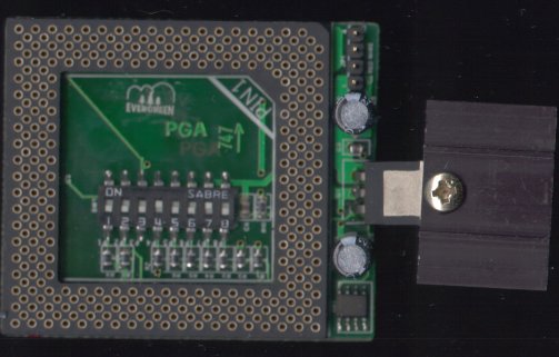
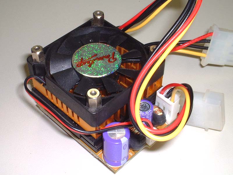
Evergreen
PowerLeap
CPU Control Panel ("CCP")
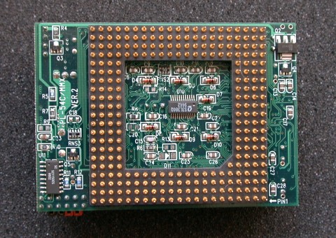
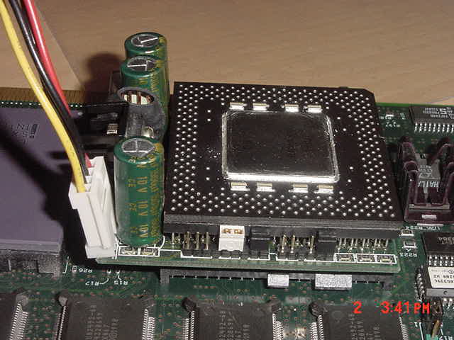
PL-54C/MMX
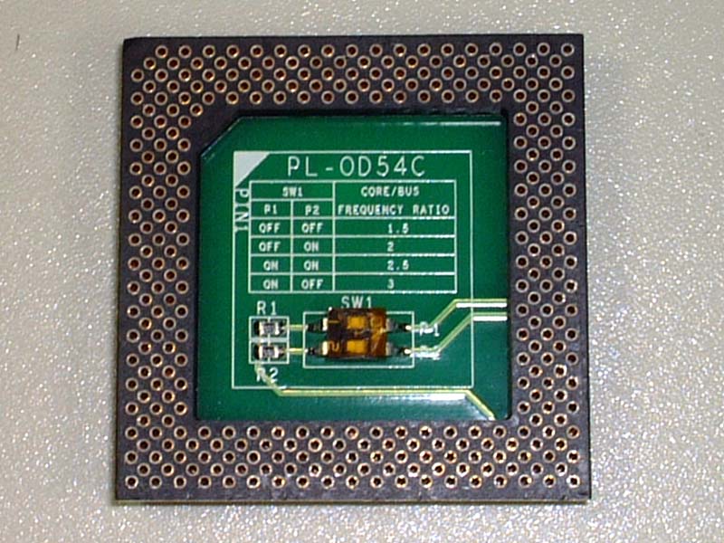
PL-OD54C
PL-MMX v2.01V
PL-ProMMX (SVRM) v4.0
PL-ProMMX (SVRM) v6.0
PL-ProMMX Plus old version
PL-ProMMX Plus v3.0
PL-ProMMX Plus v4.0
PL-K6-III
Zerus P55C-K6-S1
Madex Interposers
Upgrade Kits
Kingston
TurboChip 233
TurboChip 400
Evergreen Spectra 233/400
Buffalo HP5-MMX300L
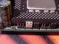
Clock and Multiplier Selection Pins (BF1 and BF0)
Intel Pentium
AMD K6
If you are planning to use AMD K6-2 CPU rated higher than 350 MHz for your
system running Windows 95B or 95C you need amdk6upd.exe.
Content created by Sandy. Edited by Major Tom.
Interposers
Evergreen
(Photo by MadMax)
Switch Settings
CLK
MUL |
P55C, M2, K6
(DUAL VOLTAGE) |
P54C, K5
(SINGLE VOLTAGE) |
| 3.5 (1.5) |
3 |
2.5 |
2 |
| P1 |
OFF |
OFF |
ON |
ON |
| P2 |
OFF |
ON |
ON |
OFF |
| P3 |
OFF |
OFF |
OFF |
OFF |
CLK
VCC |
P55C, M2, K6 6X86L
SOCKET 5 (5V) |
P54C, K5, 6X86
SOCKET 7 (3.3V) |
| P4 |
ON |
OFF |
CORE
VCC |
P54C, K5
6X86 3.3V |
K6 3.1V |
P55C, M2
6X86L 2.8V |
M2 2.5V |
| P5 |
ON |
OFF |
OFF |
OFF |
| P6 |
OFF |
ON |
OFF |
OFF |
| P7 |
OFF |
OFF |
ON |
OFF |
| P8 |
OFF |
OFF |
OFF |
ON |
DIP switch settings to run a 233MMX chip:
| P1 |
P2 |
P3 |
P4 |
P5 |
P6 |
P7 |
P8 |
| OFF |
OFF |
OFF |
ON |
OFF |
OFF |
ON |
OFF |
PowerLeap
Official Website (archived)
Troubleshooting Guide for PL-ProMMX and PL-ProMMX Plus.
US5919259 Method and apparatus for supplying power to a CPU using an adaptor card (Google)
US5938769 CPU escalating adapter with multivoltage and multiple frequency selection (Google)
CPU Control Panel ("CCP") (Windows 95/98/NT)
A software utility that displays information about your CPU, Motherboard, Chipset, and BIOS. It enables you to configure your CPU settings.
CCP 5.1.0.1 (1.32MB)
CCP 5.0.0.27 (1.31MB)
CCP 4.0.0.29A (960KB)
Last updated: Oct 2000
CCP 4.0.0.29 (960KB)
CCP 4.0.0.28 (940KB)
CCP 4.0.0.27 (680KB)
CCP4015.EXE (775KB)
CCP4013.EXE (863KB)
CCP403.EXE (837KB)
CPUPANEL.EXE (657KB)
Version 3.0, Last updated: Dec 1998. Includes support for PL/586 write-back cache.
SETUP.EXE (510KB)
Version 2.0, Last updated: Oct 1997
Using the PL-Pro/II Utility Software
User's Guide for CPU Control Panel Utility
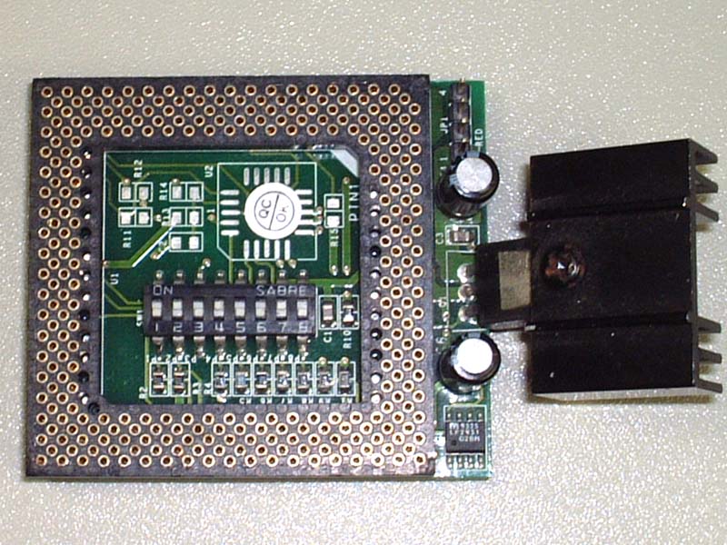
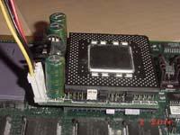
PL-54C/MMX (manual) (Photo by MadMax)
Can be used to upgrade systems with Socket 4 (original 5V Pentium) to
Socket 5/7 CPUs.
Not tested, but it should fit the Type 4 "P" and "Q" processor boards.
PL-OD54C
Upgrade for P75/90/100 systems to P133 to P200 (Non-MMX Upgrade).
Doesn't have a voltage regulator. It only provides clock multiplier jumpers for
pin BF1 which is omitted in P75/90 systems. Very simple and easy to use. You
actually don't need this interposer to upgrade P75/90 to classic Pentium
133-200, if you don't mind reworking the board
(check Peter's P90 tuning page for the
method).
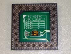
This one can be used on the Type 4 P90 "Y" complex.
Switch Settings
| SW1 |
Core/Bus Frequency Ratio |
| P1 |
P2 |
| OFF |
OFF |
1.5x |
| OFF |
ON |
2.0x |
| ON |
ON |
2.5x |
| ON |
OFF |
3.0x |
P1 connected to BF1 (Pin X34)
P2 connected to BF0 (Pin Y33)
PL-MMX v2.01V
Upgrade for Pentium 75-200 to MMX Pentium, K6 and M2.
Available CORE VCC; 3.3V, 3.1V, 2.8V, 2.1V
Maximum CORE/BUS ratio is 3.5 x (MMX 233 & K6-2 333)
This interposer won't fit on the Server 320 planar because of a large
heatsink that sits in front of the CPU sockets.
It will work on the P90 "Y" complex, but you will have to bend fins of the
LT11084 heatsink to make enough space for the interposer.
Tam's take on using this interposer with the T4 Y complex can be found
HERE.
Physical Compatibility
| PC Server 320 8640-Mxx |
No |
| Type 4 Y (P90 complex) |
Rework needed |
| PC750 6885/5886 |
? |
| SW1:P1 |
OFF |
OFF |
ON |
ON |
| SW1:P2 |
OFF |
ON |
OFF |
ON |
| RATIO |
3.5/1.5 |
3 |
2 |
2.5 |
| CPU |
P55C, M2, K6 (P54C, K5) |
| RATIO |
3 |
3 |
2 |
2 |
| CPU |
6X86, 6X86L |
|
| CLK VCC |
Socket 5 5V |
Socket 7 3.3V |
| SW1: P4 |
ON |
OFF |
|
| CORE VCC |
3.3V |
3.1V |
2.8V |
2.5V |
| SW1: |
P5 |
P6 |
P7 |
P8 |
| CPU |
P54C |
K6 *1 |
P55C |
M2 |
*1 Some of K6-233 are rated 2.2V VCC
|
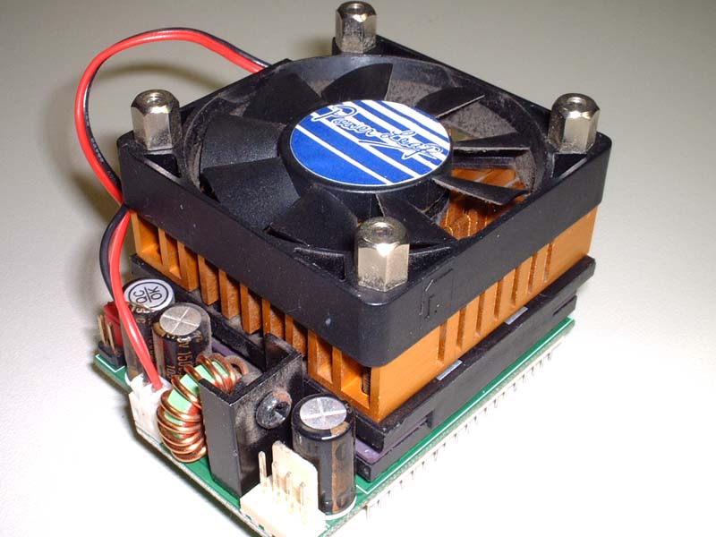
PL-ProMMX (SVRM) v4.0
It looks like PL-ProMMX Plus (below). Two
capacitors are placed around Pin 1 (front edge) but the switch block is placed
inside the Socket at CPU side like PL-MMX listed above.
Physical Compatibility
| PC Server 320 8640-Mxx |
Main CPU socket only |
| Type 4 Y (P90 complex) |
Rework needed. Not recommended. |
| PC750 6885/5886 |
Yes |
PL-ProMMX (SVRM) v6.0 (manual)
Looks similar to PL-ProMMX Plus v4.0.
No capacitors at the pin 1 side, switch block on the TOP side, inside the CPU socket.
Not tested, but it should fit to PC Server 320 (both CPU sockets), P90 complex,
PC750 and other machines.
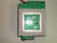
PL-ProMMX Plus old version (manual)
Upgrade for Pentium 75-200 to Intel MMX233 and (up to) K6-2/366.
Covers Core Vcc from 1.6V to 3.5V with 0.1V stepping.
JP2, Jumper blocks for Core Vcc setting, and a can type capacitor locates
in front of Pin 1. Overhang of PCB for these parts hits the Voltage regulator
in front of 2nd CPU socket of 8640/MCA planar.
NO, it does not fit to 8640-MYR. It doesn't fit to the
2nd CPU socket but DOES fit to the 1st socket.
It can be used for PC750 too.
Physical Compatibility
| PC Server 320 8640-Mxx |
Main CPU socket only |
| Type 4 Y (P90 complex) |
Rework needed. Not recommended. |
| PC750 6885/5886 |
Yes |
 |
 |
Front View (right)
Jumper Block for Core voltage settings and a capacitor in front of the
PCB may interferes with a heatsink of voltage regulator on a 8640-Mxx 2nd CPU
socket and on a Type 4 Y P90 complex.
|
 |
 |
Bottom View (left)
Silkscreened "PL-ProMMX Plus REV 2.1"
Rear View (right)
|
JP1 Settings: Clock Multiplier
|
P55C, K6, K6-2, 6x86L, 6X86MX, MII (Dual Volt), C6, P54C (Single Volt) |
6X86 *2 |
| CLKMUL |
6x *1 |
5.5x |
5x |
4.5x |
4x |
3.5x |
3x |
2.5x |
2x |
| Pin 1-2 |
Closed |
Open |
Open |
Closed |
Closed |
Open |
Open |
Closed |
Closed |
| Pin 3-4 |
Open |
Open |
Closed |
Closed |
Open |
Open |
Closed |
Closed |
Open |
| Pin 5-6 |
Open |
Closed |
Closed |
Closed |
Closed |
Open |
Open |
Open |
Open |
*1: 6x setting is not listed in the installation guide.
*2: For 6x86 (Single-Voltage) and 6X86L (Dual Voltage)
JP2 Settings: CPU Voltage and Overheating Protection
| CPU Type |
C6
WinChip |
P54C |
K6-233 *1 |
K6-200
6x86MX |
P55C
6X86L |
K6-266/300
K6-2 |
K6-3 *2 |
| Core Voltage |
3.5V |
3.3V |
3.2V |
2.9V |
2.8V |
2.2V |
1.8V |
| JP2: Pins 1-2 |
Closed |
Closed |
Open |
Closed |
Open |
Open |
Closed |
| JP2: Pins 3-4 |
Closed |
Open |
Open |
Open |
Open |
Closed |
Closed |
| JP2: Pins 5-6 |
Closed |
Closed |
Closed |
Open |
Open |
Open |
Open |
| JP2: Pins 7-8 |
Closed |
Closed |
Closed |
Closed |
Closed |
Open |
Open |
| JP2: Pins 9-10 |
Closed |
Closed |
Closed |
Closed |
Closed |
Closed |
Open |
*1 Check carefully actual voltage printed on the Chip.
Some are rated 3.2V and the others are rated
2.2V.
*2 K6-3 is listed in the guide book. I myself have
not yet tested K6-3 with this interposer.
Pins 11-12: CPU Overheating Protection)
| JP2: Pins 11-12 |
Overheating Protection |
| Closed |
Enabled |
| Open |
Disabled |
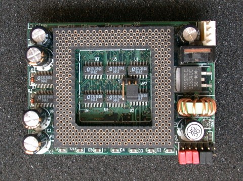
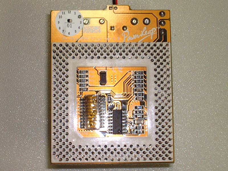
PL-ProMMX Plus v3.0 (manual)
The PCB extends only to one side of the socket, similar to version 4.0. However
the switches are on the TOP side of the board, inside the replacement CPU socket,
rather than on the underside.
See PL-ProMMX Plus v4.0 for system compatibility info.
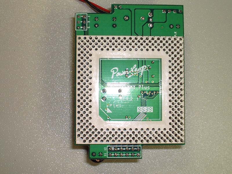
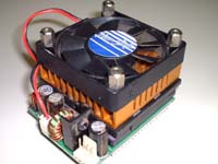
PL-ProMMX Plus v4.0 (manual)
Note: This model was later sold as just
PL-ProMMX Plus sans the version number. So you better check how it looks,
if you are planning to use it for the Type 4 "Y" P90 complex. The older version
with the same name may not fit the complex. The latest model was sold with a
heat sick/fan combo which is different compared the one pictured below.
Can be used to upgrade Pentium 75-200 systems to Pentium MMX 233, K6-2/400-450,
and other newer CPUs. Wide selection of core voltages that covers most of Intel,
AMD (except K6-III), IBM/Cyrix and IDT CPUs.
This one can be used for PC Server 320 8640 (both CPU sockets),
Y complex, and PC750 6885/6886. No capacitor nor jumper block is located on
the side with pin 1, thus the interposer doesn't interfere with the voltage
regulator heatsink of the 320 planar and Y complex.
Physical Compatibility
| PC Server 320 8640-Mxx |
Yes (both sockets) |
| Type 4 "Y" (P90 complex) |
Yes |
| PC750 6885/5886 |
Yes |
Core voltage regulation is driven by the Fairchild RC5057 DC-DC Controller.
Power Supply Connector
Connector specs: 3-pin, 3.96 mm pitch, 1.14 mm square pin. Available from many different manufacturers, e.g. JST's VH series.
Pinout of the male connector soldered to the interposer PCB (top view, pin 1 closer to the CPU socket):
|

|
| Pin | Description |
|---|
| 1 | +5 V |
| 2 | Ground |
| 3 | +12 V |
|
Switch Setting
SW1: Pins 1, 2 & 3 for Clock Multiplier
|
P55C, K6, K6-2, 6X86MX, MII (Dual Volt), C6, WinChip2, P54C (Single Volt) |
6X86 *1 |
| CLKMUL |
6x |
5.5x |
5x |
4.5x |
4x |
3.5x |
3x |
2.5x |
2x |
| Pin 1 |
ON |
OFF |
OFF |
ON |
ON |
OFF |
OFF |
ON |
ON |
| Pin 2 |
OFF |
OFF |
ON |
ON |
OFF |
OFF |
ON |
ON |
OFF |
| Pin 2 |
OFF |
ON |
ON |
ON |
ON |
OFF |
OFF |
OFF |
OFF |
SW1: Pins 4, 5, 6, 7 & 8 (Core Voltage)
| CPU Type |
C6
WinChip |
P54C
6X86 |
K6-233 * |
K6-200
6x86MX
MII |
P55C
6X86L |
K6-2/450 |
K6-266
K6-300
K6-2 |
| Core Voltage |
3.5V |
3.3V |
3.2V |
2.9V |
2.8V |
2.4V |
2.2V |
| SW1: Pin 4 |
ON |
ON |
OFF |
ON |
OFF |
OFF |
OFF |
| SW1: Pin 5 |
ON |
OFF |
OFF |
OFF |
OFF |
OFF |
ON |
| SW1: Pin 6 |
ON |
ON |
ON |
OFF |
OFF |
ON |
OFF |
| SW1: Pin 7 |
ON |
ON |
ON |
ON |
ON |
OFF |
OFF |
| SW1: Pin 8 |
OFF |
OFF |
OFF |
OFF |
OFF |
OFF |
OFF |
* Check carefully actual voltage printed on the CPU label.
(there are two types in K6-233, different core Vcc)
* You can set Core Voltage to another value not listed in above diagram.
From 1.30 V to 2.00V by 0.05V stepping and from 2.0V to 3.5V by 0.1V stepping.
SW1: Pin 10 (CPU Overheating Protection)
| SW1: Pin 10 |
Overheating Protection |
| ON |
Enabled |
| OFF |
Disabled |
SW1: Pin 9 - No comment for Pin 9 in the associated Manual. But there
is a instruction for this pin SW in Installation Guide PDF for PL-K6-III. Don't
know if Pin 9 actually works for this model or not. At least, in all sample
diagrams for CPU setting show this pin in OFF position.
From PL-K6-III PDF:
SW1: Pin 9 (Pin AL-1 Compatibility) Pin 9 of SW1 lets you
enable/disable the pin signal for split-voltage detection. This function
provides compatibility for certain HP Vectra and Biostar systems that check the
signal.
For split-voltage CPUs, certain HP Vectra (VL100 and VL5/133
Series 5 DT) systems and certain Biostar motherboards (8500TUD and M5ALA) check
for the presence of a signal from pin AL-1. Unfortunately, these systems use
the AL-1 pin signal differently: the signal must be disabled in order for the
HP Vectra systems to function properly, while the Biostar motherboards need to
detect the signal in order to boot.
If your HP Vectra or Biostar system does not run properly with the
PL-K6-III installed, try using pin 9 of the SW1 DIP switch to turn the AL-1 pin
signal on/off. Pin 9 is set to ON by default--this setting allows Biostar
systems to detect the pin signal and boot. For HP Vectra systems, changing the
switch setting to OFF will disable the signal and allow the system to function.
Most systems (including most HP Vectra systems and Biostar motherboards) will
be unaffected by the pin AL-1 setting.
Pin 9: Pin AL-1 Compatibility
| SW1: Pin 9 |
AL-1 Compatibility |
| ON |
Pin Connected |
| OFF |
Pin Disconnected |
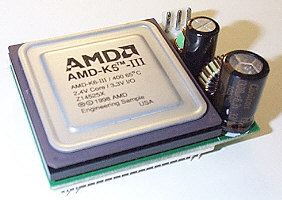
PL-K6-III
A further development of the PL-ProMMX Plus interposer. It brings official support for the AMD K6-III chips.
Multiple different revisions:
PL-K6-III/98 version 1.0
PL-K6-III version 2.1
PL-K6-III version 2.2
PL-K6-III version 2.3
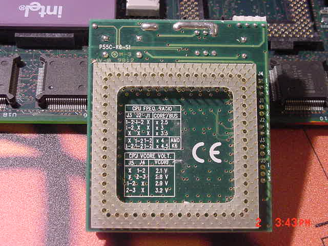
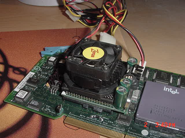
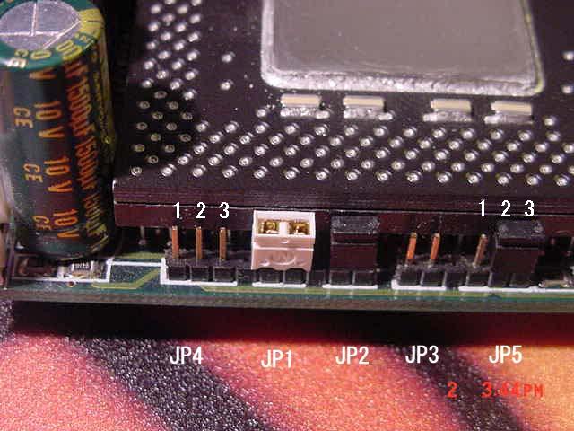
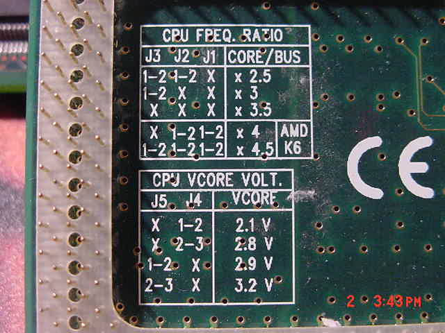
Zerus P55C-K6-S1
(Photos by Jim Hall, Explanation by Jim)
"For those of you who haven't seen this upgrade, it consists of an
interposer similar to the Madex, with a plug for a power tap used on 3 1/2"
clone style floppy drives to handle the power requirements of the Intel (or
any pin compatible) CPU. The cooling fan also draws its power from the same
source."
Exactly the same product was also sold in Japan before. it was named as
"Multimedia CPU Upgrade Kit". It was made of Taiwan and marked as "CE". I
don't know this "CE" logo which can be seen many computer products manufactured
in Taiwan.
 |
 |
 |
| 1) Close View |
2) Bottom View |
3) On the Type 4 "Y" |
 |
 |
 |
| 4) Jumper Block |
5) Jumper Settings |
6) Jim's Proud 90MHz M95 |
Specifications
Socket 5 or 7
Voltage Supplied: 2.2V, 2.8V, 2.9V, 3.2V
Current rate: 15A for P55C-K6-S
Connection: 320 pin SPGA
|
Multiplication Jumper Setting
| JP1 |
JP2 |
JP3 |
Speed |
| OPEN |
1-2 |
1-2 |
2.5x |
| OPEN |
OPEN |
1-2 |
3.0x |
| OPEN |
OPEN |
OPEN |
3.5x |
| 1-2 |
1-2 |
OPEN |
4.0x |
| 1-2 |
1-2 |
1-2 |
x 4.5 |
| 1-2 |
OPEN |
1-2 |
5.0x |
| 1-2 |
OPEN |
OPEN |
5.5x |
| 1-2 |
1-2 |
OPEN |
6.0x |
x 6.0 is not documented, but theoretically...
|
|
Vcore Voltage setting
| JP5 |
JP4 |
Vcore |
| OPEN |
1-2 |
2.2V |
| OPEN |
2-3 |
2.8V |
| 1-2 |
OPEN |
2.9V |
| 2-3 |
OPEN |
3.3V |
Combination of JP5/OPEN and JP4/1-2 listed topmost column is printed as
2.1V on the PCB but supplement sheet says it was changed to 2.2V on -S1.
|
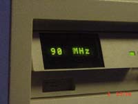
3.3V single voltage for I/O and Core is not designated. Thus Jim set
Core voltage to 3.2V and put his classic Pentium P166 with 3x speed jumper
setting and set it on his Y complex. Y complex has 60 MHz OSC so
his system actually run at 180 MHz.
Report to the news group from Jim Hall:
"OK, ran a little windows program called CPU id, by Alexander
Berezkin. It identifies the CPU as an Intel Pentium, brand name Genuine Intel.
Type ID = 0
Family ID = 5
Model ID = 2
Stepping ID = 12
Clock Frequency, Internal = 180 MHz"
Madex Interposers
Information about Madex Interposers for Socket 5 and 7 systems:
English: Product Page, Jumper Settings
German: Product Page, Jumper Settings (has some extra info)
Upgrade Kits
Kingston
TurboChip 233
(guide)
Kingston TurboChip 233 uses Intel MMX233 CPU.
Features:
- Powerful Intel® MMX enhanced microprocessor running at
- 233MHz processing speed.
- 32KB Level One (L1) Cache
- Onboard voltage regulator to interface with either 2.8V or 3.3V system
motherboard automatically.
- Supports multimedia extensions instructions
- "Plug and Play" installation. No software drivers to install.
Unfortunately TurboChip 233 does not have CPU speed jumper and it will
automatically set the clock multiplier to 3.5x. It is supposed that TurboChip
233 may not run on Y complex. Any experience?
TurboChip 200
TurboChip 200 uses AMD K6 200 MHz. Most possibly, It will be kicked out by
system BIOS of Y complex.
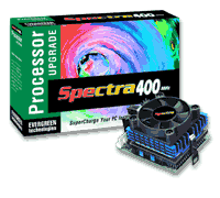
TurboChip 400
(guide)
Turbochip 400 uses K6-II/400 CPU. Needless to say it's incompatible with
Type 4 "Y" complex.
But it may run in PC Server 320/520 or PC750 6886.
Evergreen Spectra 233
(manufacturer)
Evergreen Spectra Install Disk (zipped image) (thx to Christian Holzapfel)
Not sure which CPU this unit uses, Intel MMX233 or K6. Anyway "233" means
it may not work on Y complex.
There were several models rated 300 MHz to 400 MHz using K6-II CPUs like
Kingston TurboChip.
I'm not sure but it seems Spectra upgrades do not have clock multiplier
jumpers and they automatically set it to Max rating provided with the CPU used.
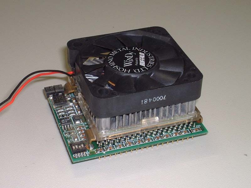
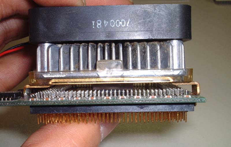
Buffalo HP5-MMX300L
CPU accelerator by Buffalo. Mobile MMX300 assembled on a PCB for PGA Socket 5/7.
Intel CPU is used for this accelerator. But Y complex can't boot with it.
Works fine for 6886 planar so far.
Clock and Multiplier Selection Pins (BF1 and BF0)
Intel Pentium (from Intel Documents)
Multipling Pins
| CPU |
Signal |
Pin |
Active Level |
Synchronous/
Asynchronous |
Internal Register |
| P54C |
BF0 |
Y33 |
HIGH |
Synchronous/RESET |
Pull-up |
| BF1 |
X34 |
HIGH |
Synchronous/RESET |
Pull-up |
| P55C |
BF0 |
Y33 |
N/A |
Synchronous/RESET |
Pull-down |
| BF1 |
X34 |
N/A |
Synchronous/RESET |
Pull-up |
BUS Frequency Selection for P54C
| BF1 |
BF0 |
Bus/Core Ratio |
Core Frequency (MHz) |
External Bus
Frequency (MHz) |
| 0 |
1 |
1/3 |
200/180/150 |
66/60/50 |
| 0 |
0 |
2/5 |
166/150/125 |
66/60/50 |
| 1 |
0 |
1/2 |
133/120/100 |
66/60/50 |
| 1 |
1 |
2/3 *1 |
100/90/75 |
66/60/50 |
|
| 0 |
0 |
1/4 *2 |
266/240/200 *2 |
66/60/50 *2 |
*1 Default BUS/Core ratio is 1/2 for P54C.
*2 4x mode was not officially announced by Intel but it is told that some
Pentiums with marking of SXxxx and SYxxx have this special Core/BUS ratio.
Early Pentiums (P90 & P75) do not have BF1.
BUS Frequency Selection For P55C
| BF1 |
BF0 |
Bus/Core Ratio |
Max Bus/Core
Frequency (MHz) |
Min Bus/Core
Frequency (MHz) |
| 0 |
1 |
1/3 |
66/200 |
33/100 |
| 0 |
0 |
2/5 |
66/166 |
33/83 |
| 1 |
0 |
1/2 (*1,*2) |
N/A (2) |
N/A (2) |
| 1 |
1 |
2/7 |
66/233 |
33/177 |
*1 This is the default bus to core ratio for the Pentium processor with
MMX technology. If the BF pins are left floating, the processor will be
configured for the 1/2 bus to core frequency ratio.
*2 Currently, there are no products that support these bus fractions.
AMD K6 (from AMD K6-2 Data Sheet)
BF[2:0] (Bus Frequency) - Inputs, Internal Pullups
Summary: BF[2:0] determine the internal operating frequency of the processor.
The frequency of the CLK input signal is multiplied internally by a ratio
determined by the state of these signals as defined in the Table below.
BF[2:0] have weak internal pullups and default to the 3.5 multiplier if left
unconnected.
Processor-to-Bus Clock Ratios
BF[2:0]
State |
Processor-Clock
to Bus-Clock Ratio |
| 100b |
2.5x |
| 101b |
3.0x |
| 110b |
2.0x or 6.0x* |
| 111b |
3.5x |
| 000b |
4.5x |
| 001b |
5.0x |
| 010b |
4.0x |
| 011b |
5.5x |
* The ratio selected is dependent on the stepping of the Model 8. The 2.0x
ratio is supported on the Model 8/[7:0], whereas the 6.0x ratio is supported
on the Model 8/[F:8].
Sampled: BF[2:0] are sampled during the falling transition of RESET.
They must meet a minimum setup time of 1.0 ms and a minimum hold time of two
clocks relative to the negation of RESET.
|