|
The IBM RS/6000
processor: Hardware Overview
Pseudorandom BIST methodology
and implementation for IBM RS/6000 processor
CPU (RIOS 1.0 - 10 Chips)
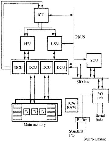
Cost Reduced CPU (RIOS .9 - 8 Chip)
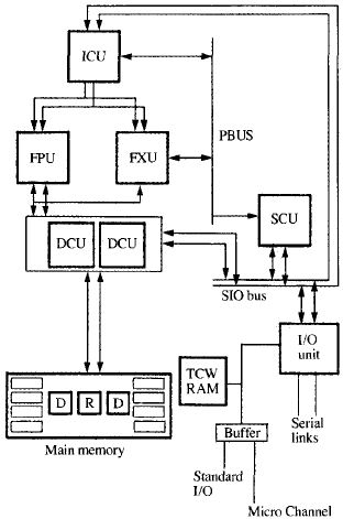
Cost-Reduced CPU (RIOS .9 / 8 Chip)
One of the goals of this design was to use a common chip set
to produce a family of processors with varying cost and
performance. This was accomplished by designing the FXU,
DCU, and SCU in such a way that they can operate with two
DCUs as well as with four. This system configuration is
illustrated in Figure 4. Because the chips are common to the
two versions, they can be sorted so that faster chips are
used in the high end and slower ones in the entry-level
configurations. In this way, sorting for high speed is
achieved without sacrificing the overall yield.
This configuration has a lower cost for two reasons. First,
it has only two data-cache chips rather than four. Second,
it requires a minimum of one memory card rather than two.
(This is because two DCU in the cost reduced CPU have a
two-word memory interface
compared to four DCUs in the full CPU, which have a
four-word interface. Consequently, some of the
bit-scattering features described for the full-size CPU do
not apply to the cost-reduced CPU.) To accommodate the
smaller cache size and narrower memory bus width, the
D-cache line size is reduced to 64 bytes. In the cost
reduced CPU, fixed- and floating-point data buses are dotted
together. In addition, the DCU sends the data to reload the
I-cache over the SIO bus rather than having a dedicated
I-cache reload bus to the ICU.
Memory Cards
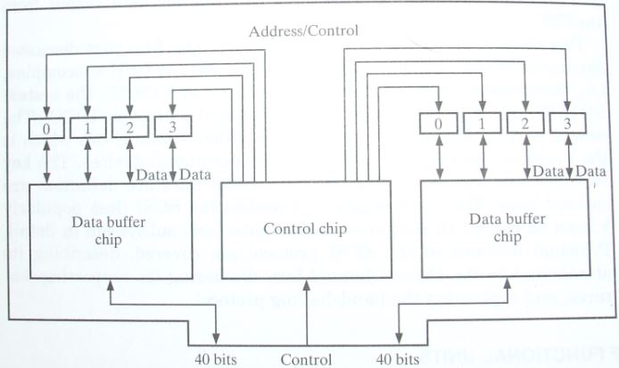
RISC System/6000 memory cards implement a four-way
interleaved design in order to provide two words of data
every machine cycle from each memory card. A minimum of two
memory cards is required to support the four-word memory bus
to the CPU (Figure 1).
The interleaving is performed by two data-multiplexing chips
(D) and one control chip (R) on the memory cards. The memory
cards accept generic read/write instructions and generate
the required read/write, refresh, and page-mode read/write
signals for a variety of DRAMs. The memory cards can buffer
up to four instructions and 16 words of write data. Using
standard modular SIMM packages for the DRAMs provides
flexibility in memory capacity and cost. RS/6000 memory
cards can support both 1-megabit and 4-megabit DRAMs. The
SIMMs are 1, 2, or 4 MBs. There are eight SIMM sockets per
memory card, yielding 8-, 16-, or 32-Mbyte memory cards. A
system can have 2 to 8 memory cards providing 16 MBs to 256
MBs of total memory. With the 4-Mbit DRAM technology, the
memory card capability can be increased to 64 MBs, and the
total memory capability can be increased to 0.5 GBs. Bit
scattering is implemented to guarantee that no more than one
bit of a 40-bit ECC word is stored in an individual DRAM.
Accordingly, the bit-steering circuitry in the DCU can
detect and correct errors caused by a single bad by-four
DRAM chip and still have additional error protection due to
ECC.
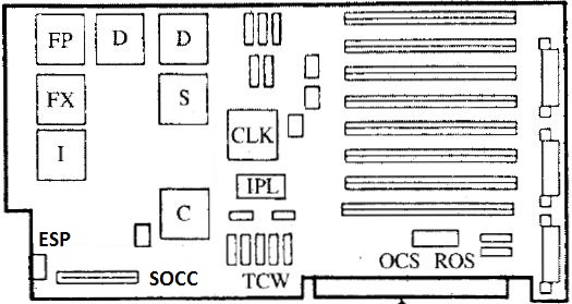
Chipset Work RIOS 1.0
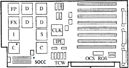
FP - Floating Point Unit (FPU)
FX - Fixed Point Unit (FXU)
D - Data Cache Unit (DCU)
I - Instruction Cache Unit (ICU)
S - Storage Control Unit (SCU)
C - Input / Output Unit (IOU)
CLK - Clock
TCW - Translation Control Words (TCW) buffer
OCS - On-Card Sequencer (OCS)
ROS -
IPL -
This is a RIOS 1.0 version CPU planar. This planar supports
a 4 memory card system, so it has 4ea DCU.
Note that the left (out-board) IOU (marked C *) may either
be totally missing (just solder pads), a empty socket, a
socketed IOU chip, or a soldered-in IOU chip. Normally, if
there is no socket or chip in C * position, the top most
SOCC slot is not installed (solder pads for SOCC slot only).
Chipset Work RIOS
0.9
FP - Floating Point Unit (FPU)
FX - Fixed Point Unit (FXU)
D - Data Cache Unit (DCU)
I - Instruction Cache Unit (ICU)
S - Storage Control Unit (SCU)
C - Input / Output Unit (IOU)
CLK - Clock
TCW - Translation Control Words (TCW) buffer
OCS - On-Card Sequencer (OCS)
ROS -
IPL -
This is a RIOS 0.9 version CPU planar. This planar supports
a 2 memory card system, so it has 2ea DCU.
Note that the left (out-board) IOU is totally missing (just
solder pads). The top most SOCC slot is not installed
(solder pads for SOCC slot only).
Just to show the bare truth, different FRUs may be quite
different...
7012-340 CPU Planar ID 37
(33 POWER) 43G0716, 00G3149 dated 9231
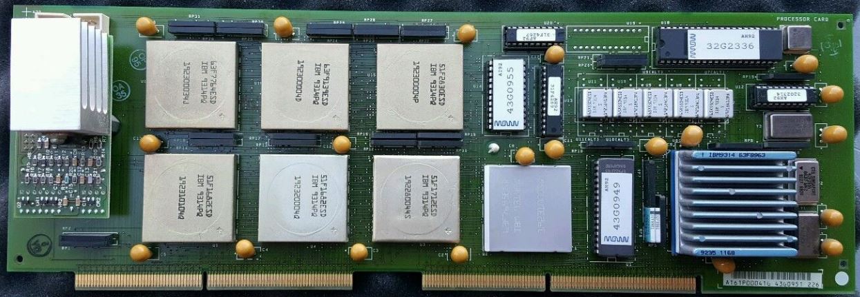
U1 43G0949 uCode
U2 63F7695 CLK
U3 51F1712 SCU
U4,5 51F6832 (DCUs)
U6 63F8963 IOU
U7-11 65X5504 Metal cubes - TCW
U14 43G0955 IPL?
U15 51F2830 ICU
U16 63F9139 FXU
U17 63F7764 FPU
U18 32G2336 OCS ? 8051 size
U20, 13 ROS?
7012-340 CPU Planar ID 37
(33 POWER) 52G4314, 52G4190 dated 9317
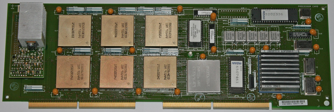
U1 65G7461 uCode
U2 63F7695 CLK
U3 33G0564 SCU
U4,5 33G5673 (DCUs)
U6 63F8963 IOU
U7-11 65X5504 Metal cubes - TCW
U14 52G4315 IPL?
U15 50G5736 ICU
U16 50G5730 FXU
U17 50G5733 FPU
U18 32G2336 OCS ? 8051 size
U20, 13 ROS?
Storage Control Unit (SCU)
The SCU is the central system controller [9].
All of the communication between CPU (ICU, FXU, DCU), main
memory, and I/O is arbitrated by the SCU. The CPU sends
I-cache reload, D-cache reload and D-cache storeback
requests to the SCU over the PBUS, and the SCU generates the
appropriate memory-control signals. The SCU is the bus
master for the memory and SIO buses. It controls the
interface between D-cache and system memory, and oversees
DMA operations between main memory and the I/O unit. The SCU
provides a data path for I/O loads and stores between the
CPU and I/O unit via the PBUS and SIO bus. The SCU also
forms an interface to the IPL ROS. Memory scrubbing is
controlled by the SCU, and memory errors detected by the DCU
are recorded by the SCU. The SCU contains the bank
configuration registers, which indicate the size and
starting point of each bank of storage in system memory.
I/O Unit (IOU)
The I/O unit contains an I/O channel controller (IOCC) and
two serial link adapters (SLAs). The IOCC generates a Micro
Channel interface, and the SLAs provide an interface to
optics cards that drive fiber-optic links. Support for this
high-speed optical link is planned for a future release. The
data interface between CPU/system memory and the I/O unit is
via the two-word SIO bus. Micro Channel has a one-word
address bus and a one word data bus. Data transmission
between an SLA and the optics cards are via one-byte
interfaces.
The IOCC supports an I/O architecture geared for
performance, robustness, and error recoverability [11]. The
main function of the IOCC is to transfer data between system
memory and adapters on the Micro Channel. The CPU can
transfer data to/from adapters
using I/O load and store operations, and adapters can
transfer data to/from system memory using DMA. The IOCC
supports both DMA bus masters and DMA slaves. All data
transfers support address-protection mechanisms to provide
data security. Up to 15 DMA channels and 16 levels of
interrupts are supported by the IOCC. The Micro Channel
Architecture features include streaming data, address and
data parity, and synchronous exception reporting (I/O
loads/stores cause precise interrupts like regular
loads/stores) [12]. With the new streaming-data mode,
multiple data packets can be transferred within one bus
envelope. This is accomplished by sending a starting address
and then transferring a block of data consisting of multiple
consecutive data packets. This is in contrast to the regular
mode, where an address is required for every data transfer.
This amortizes device selection overhead across the entire
packet and nearly doubles the performance for large data
bursts [12]. Precise I/O load/store interrupts improve error
recoverability.
The SLA implements the serial I/O architecture, which
supports point-to-point connections where two RS/6000
machines communicate with each other via optical fibers
[13]. The SLA receives the data from the CPU, puts it into
10-bit packets, and transmits the packets to the optics
card. The optics card serializes the data and feeds it to a
fiber-optic link. The SLA also supports I/O loads/stores
to/from the CPU. Each SLA contains two 256-byte data buffers
to transfer data between the SIO bus and the optics card,
and one 16-word tag table to provide pointers to a
system-memory buffer for DMA operations.
Serial Optical Channel Converter
(SOCC)
All deskside and larger IBM RISC System/6000 computers have
at least one SOCC slot. That is to say, the RISC system
models 220 and 300 series have no optical slots, the
deskside 500 series has one optical channel slot, and the
900 rack series two. Because of the speed of this interface
it is necessary to locate optical slots on the CPU planar
rather than on the I/O planar where MicroChannel slots are
located. This design also ensures that large amounts of
optical network traffic do not swamp the bandwidth of the
MicroChannel I/O bus. Into each slot plugs an SOCC card.
Each card has four unidirectional links (half duplex), with
two links working together to form a port. Each port can be
connected to a router manufactured by Network Systems Corp.
(Data Exchange Box - "DX Box", no further info at this time)
The Network Systems router can be viewed as an optical
junction box interconnecting the SOCC-connected RISC
systems. The router also has an FDDI network output and,
optionally, an IBM mainframe channel connection. Using the
SOCC configuration actual RISC system to RISC system raw
transfer rates of 220 megabits per second are possible.
Architecturally, speeds of up to 400 megabits per second
could be driven through the optical channel. The software
interface that sits on top of the physical SOCC is TCP/IP
and
provides the full range of TCP/IP commands and programming
interfaces available to the user and programmer.
Pseudorandom Built-In Self-Test
(BIST)
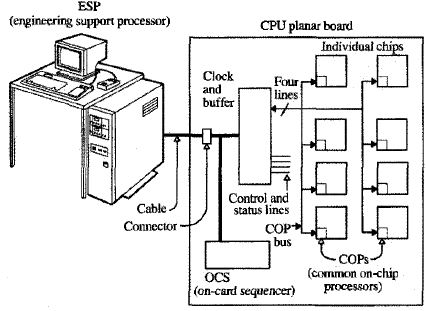
The BIST architecture for the CPU board is shown in Figure
1. It consists of four components that are presented in
detail in the rest of this paper, the common on-chip
processor (COP); the serial bus linking the chips (COP bus);
the on-card sequencer (OCS); and the engineering support
processor (ESP).
Common On-chip Processor (COP)
The COP is a technology independent processor
that controls the built-in self-test sequence. There is a
COP on every CPU chip, and a COP takes less than 3 percent
of a CPU chip in this particular implementation. The COP
communicates with the outside world via a four-bit serial
bus according to a simple bus protocol. Together with the
on-card sequencer, the COP isolates faulty CPU chips.
Together with the engineering support processor, the COP
also aids in the bring-up and test of CPU chips not
previously tested elsewhere.
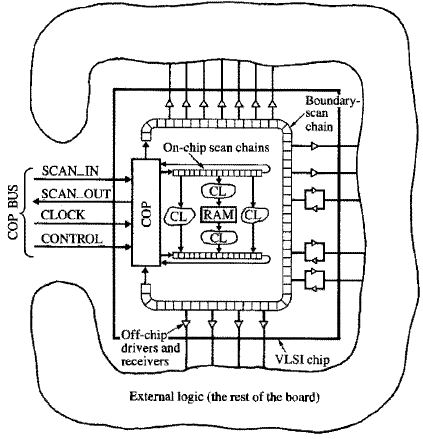
Note: "The external
interface of the COP is the four-pin serial COP bus.
Commands issued on this bus by either the on-card sequencer
or the engineering support processor are processed by the
COP and appropriate action is taken. The bus protocol
supports both broadcast mode and individual addressing of a
chip."
Engineering Support Processor (ESP)
The ESP is a stand-alone processor used for
verification, bring-up, and debug. Unlike the OCS, which is
part of the product, the ESP is not shipped with the
product. It consists of an IBM RT System equipped with a COP
bus interface adapter and the application software that
controls its operation. The COP bus interface adapter acts
as a protocol converter between the native AT bus of the RT
and the serial COP bus of the RISC System/6000 CPU board.
The ESP is intended to operate at a debug station in
manufacturing or in a laboratory; it can be up to 30 meters
away from the CPU board under test.
Because the ESP implements the full set of COP commands, it
can run all the functions of the OCS. The additional
functions of the ESP allow it to aid in the isolation of
faults during system verification and debug, operations that
require larger memory and disk storage than are available in
the OCS:
* Control of architectural verification programs.
* Hardware debug for chip, board, and system.
* Software debug of the operating system.
The ESP software runs under the AIX operating system and
consists of 25,000 lines of C code. It takes about 15 MBs of
file space on the RT and runs in 800 KBs of RAM. The
interface makes extensive use of windowing and can be
tailored by the user.
To support a new chip with a COP, only three parameters need
to be passed to the ESP software: the LSSD scan string
tables, the embedded memory definition, and the new screen
definition for the user. Once the new breakpoints are set,
the debug process can start exactly as it does for any other
chip with a COP. This remarkable consistency has resulted in
a reduction in CPU chip bring-up time from a few months to a
few weeks.
On-Card Sequencer (OCS)
The OCS is an 8-bit 8051 microcontroller with a
4-KB on-chip ROM and 128 (KB?) bytes of on-chip RAM. The ROM
stores the "seed-good" signature pair for a pseudorandom
test sequence. The good signature is obtained either through
simulation or by using a "golden model" approach. Both seed
and signature for a sequence are 31 bits long; hence,
several hundred can be stored in the 4-KB on-chip ROM. For
system function, the OCS addresses external memory on the
CPU board for system operation and maintenance: 64 KB of ROM
and 16 KB of nonvolatile RAM. It responds to the reset
button on the operator panel and reports errors on the
operator panel display.
The main function of the OCS is CPU self-test and reset.
Because the OCS contains both seed and good signatures for a
test sequence, it can control an entire self-test sequence
by sending the proper commands to the COP of each chip. At
power-up, after both supply voltage and system clock are
stable, the OCS broadcasts a set of commands from its
on-chip ROM onto the COP bus. First, all three-state output
drivers for the CPU chips are disabled, thus electrically
isolating each chip from its neighbors. From this point on,
all CPU chips operate in parallel. The following sequence is
executed:
1. Initialize the COPs.
2. Initialize all embedded memories.
3. Test embedded memories.
4. Self-test the DC logic.
5. Self-test the AC logic.
After each operation, the OCS polls the individual COPs. If
all signatures match the stored ones in the OCS ROM, the CPU
is reset for system initialization.
If the signature generated by a sequence does not match the
"golden" one in the OCS ROM, a suitable error code is
flashed on the operator panel display. The size of the
sequence and the number of stored golden signatures
determine the resolution of the OCS self-test. For example,
self-test can identify a specific failing embedded memory on
a chip.
Each test operation in the above sequence may involve
several million system cycles. Regardless of how many cycles
are executed, the test output data is always compressed to a
31-bit signature. Since seed and signature are less than
four bytes each, the speed and bandwidth of the four-pin
serial COP bus are adequate.
The CPU board self-test unequivocally identifies all failing
chips. Since the I/O circuitry is not exercised, the
chip-to-chip connections must be tested later (during the
functional self-test for the entire system).
Note: Not all CPU cards
/ planars have a discrete OCS.
|