
Source: IBM Personal Systems Technical Solutions, Oct 1992 (G325-5019-00), pages 9-13
Author: Jim Paolantonio, IBM Corporation, Boca Raton, Florida
Programmable Option Select (POS) registers are an innovative feature in
PS/2 Micro Channel systems that eliminate the need for manual switches on the
system board and on adapter cards. As the name implies, these registers must be
programmed. This article discusses programming the POS registers on the XGA
Display Adapter. It gives details about the contents of each register, and
shows how the system puts these contents to use.
The XGA Display Adapter provides high-resolution graphics (1024 x 768 with
256 colors) along with Video Graphics Array (VGA) mode operation. In the
Extended Graphics Array (XGA) graphics mode, the XGA adapter's graphics
coprocessor supports hardware drawing assist functions: BitBLT (Video Bitmap
Block Transfer), line drawing, and area fill. These functions are optimized for
use with the Microsoft Windows and OS/2 Presentation Manager graphical
operating environments.
The XGA video subsystem programming interface has a complex set of hardware
registers with selectable Input/Output (I/O) and memory mapped addresses. These
registers and addresses are as follows:
- 5 Programmable Option Select (POS) registers
- 16 direct I/O registers
- 128 indirect (indexed) I/O registers
- 128 memory-mapped graphics coprocessor registers
- 1 MB video buffer memory mapped addresses
It is impossible to discuss in a single article how all these registers are
programmed. This article concentrates on the functions within the five POS
registers used by the XGA Display Adapters.
POS Register Concept
During Power-On Self Test (POST), each adapter's POS registers are
programmed with information about the unique features (the configuration) of
that adapter. POST reads an adapter's unique POS ID, which is hard-coded into
the adapter's POS registers. The POS ID code (similar to a product's bar code)
identifies the type of adapter resident in a Micro Channel slot. During setup,
the POST process, in conjunction with the system configuration utilities,
configures each adapter by programming its POS registers.
The adapters and the system board each have a set of up to eight POS I/O
addresses between 100h (where h denotes hexadecimal) and 107h. Depending on the
number of unique functions incorporated, a specific adapter may not need to
implement all eight POS registers.
The contents of the POS registers can be accessed by using the System
Services POS BIOS call INT 15 (software Interrupt 15) with AH= C4h. Although
application programs never write to the POS registers, they may need to read an
adapter's POS registers. The POS registers can contain pertinent information
required to run an application.
The XGA POS Registers
The XGA video subsystem hardware interface contains its own distinct POS
Registers 0, 1, 2, 4, and 5, which respectively have I/O addresses 100h, 101h,
102h, 104h, and 105h. These registers, which are set up only once (during
POST), contain information about the locations of the XGA subsystem registers
and the video display buffer.
POS Registers 0 and 1
XGA POS Registers 0 and 1 contain the low and high bytes, respectively, of
the XGA adapter's POS ID. The currently allocated XGA adapter POS ID is 8FDBh.
(Additional POS IDs, 8FD8 through 8FDA, are reserved for future versions of
XGA.) Figure 1 shows how POS ID 8FDBh is situated in POS Registers 0 and 1.

Figure 1. Contents of XGA POS Registers 0 and 1: Subsystem
Identification
The system configuration utilities use the XGA adapter's POS ID to locate
the corresponding XGA Adapter Description File (ADF). The ADF contains specific
information for programming the XGA hardware registers. Figure 2 shows the ADF
for the XGA Display Adapter.
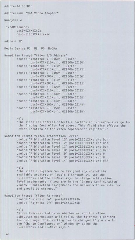
Figure 2. Adapter Description File for the XGA Display
Adapter
I/O Addressing and Memory-Mapped Addressing
Before describing POS Register 2, it is necessary to explain I/O and
memory-mapped addressing. The Intel microprocessor architecture has two
distinct modes for addressing devices. The first mode is I/O addressing. The
real-mode DOS environment has 64 KB of I/O addresses that are available for
addressing devices in the system. In this mode, when the processor addresses a
device, it uses the Intel assembly language IN instruction to read the XGA I/O
registers, and the OUT instruction to write to those registers.
In memory-mapped addressing mode, the processor uses Memory Read and Memory
Write instructions to communicate with system memory, diskette drives, and hard
disk drives. Memory mapped addresses total 1 MB in the real-mode DOS
environment. The XGA Display Adapter has memory mapped addresses associated
with its video RAM and graphics coprocessor.
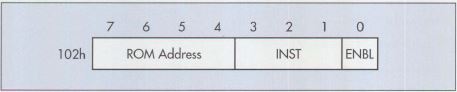
Figure 3. Contents of XGA POS Register 2: ENBL Bit, Instance,
and ROM Address
POS Register 2
The primary purpose of XGA POS Register 2 is to provide a card-enable
function. This function permits the XGA adapter to be disabled - essentially,
turned off- in the Micro Channel slot, so that it does not respond to its
assigned I/O addresses and memory-mapped addresses. In addition, POS Register 2
contains the XGA adapter's instance. Because there can be up to eight XGA
adapters present in the system, the instance (a number between 0 and 7)
distinguishes one XGA adapter from another. POS Register 2 also houses the
memory-mapped address range selector for the ROM on the XGA adapter that
contains program code. Figure 3 shows the contents of POS Register 2.
ENBL
In POS Register 2, when the ENBL bit (bit 0) is a 1, the XGA video subsystem
is enabled and responds to all non-POS addresses (that is, to all XGA direct
and indirect I/O addresses, and to coprocessor and video RAM memory-mapped
addresses). There are 16 direct I/O registers. These registers contain indexes
to 128 indirect registers. Direct and indirect registers are discussed at the
beginning of this article. When the ENBL bit is a 0, the XGA subsystem responds
only to POS register addresses.
INST
The INST field, in bits 1 through 3 of POS Register 2, defines an XGA
adapter's instance. Each XGA instance has a unique set of direct and indirect
I/O addresses, as well as coprocessor and video RAM memory-mapped addresses.
The instance also is used to locate which of the eight blocks of 128 addresses
(refer to Figure 4) is assigned to the XGA coprocessor registers.
ROM Address
The XGA Display Adapter has a Read-Only Memory (ROM) containing the POST
code that initializes the XGA registers. This ROM occupies the first 7 KB of an
8 KB memory address block. In POS Register 2, the ROM Address field (bits 4
through 7) specifies which of 16 possible 8 KB blocks of memory-mapped
addresses has been assigned to this XGA adapter. The remaining upper l KB of
address space in this same block is reserved for eight instances of the 128 XGA
coprocessor memory-mapped registers.
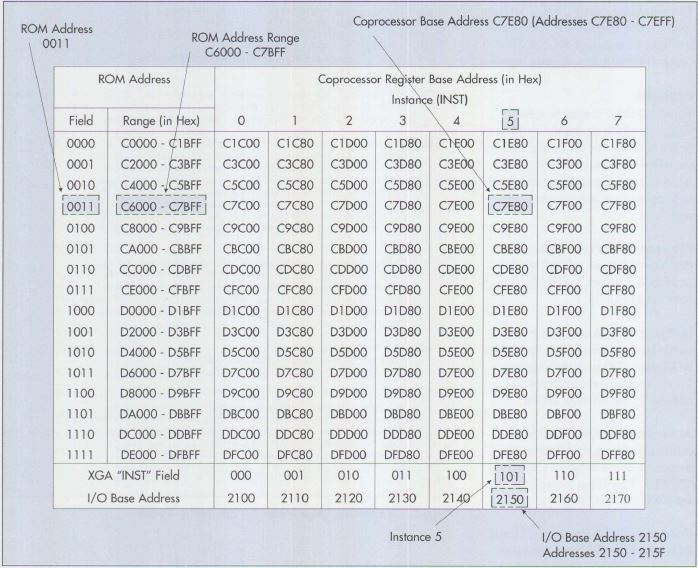
Figure 4. XGA I/O Address and Memory-Mapped Address Blocks
Example
To use all these concepts, refer to Figure 4, which shows the
correspondence between the XGA instance and the ROM address, and between the
XGA I/O register and the video ROM and coprocessor memory-mapped addresses.
The example in Figure 4 assumes that XGA instance 5 (INST=l0lh) and ROM
Address 3 (0011h) have been selected.
In Figure 4, XGA instance 101h yields base address 2150h for the 16 XGA
direct I/O register addresses. The 16 registers extend from I/O address 2150h
through 215Fh.
At the same time, ROM address 001lh provides a ROM memory mapped address
range of C6000h to C7BFFh. This is the lower 7 KB of the 8 KB address
block.
Combining XGA instance 101h and ROM Address 001lh yields a base address of
C7E80h for the 128 memory-mapped coprocessor registers. These registers reside
within the upper 1 KB of the same 8 KB address block, and they extend from
address C7E80h through C7EFFh.
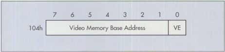
Figure 5. Contents of POS Register 4: Video Memory Base Address
POS Register 4
POS Register 4, shown in Figure 5, contains the base address of XGA video
memory.
Video Memory Base Address
The XGA Display Adapter contains up to l MB of video memory. The seven most
significant bits of the base address of the XGA memory are defined in bits 1
through 7 of POS Register 4. The three least significant bits of the base
address of XGA memory are defined in the three XGA instance bits in POS
Register 2. These two fields of bits are concatenated to define a 10-bit video
memory address located on a 4 MB address boundary.
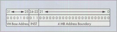
Figure 6. Finding the Base Address of XGA Video Memory
Figure 6 shows how to determine the video memory address. In Figure 6, bits
25 through 31 contain a copy of the information in bits I through 7 of POS
Register 4. These seven most significant bits of the video memory address are
set to binary 4 (0000100b). Also in Figure 6, bits 22 through 24 contain a copy
of the information in the XGA instance (bits 1 through 3 of POS Register 2).
These three least significant bits of the video memory address are set to
binary 3 (01lb).
Together, bits 22 through 31 in Figure 6 constitute the 10-bit video memory
address. Next, bits 0 through 21 in Figure 6 contain zeros. These represent the
4 MB address boundary. Finally, bits 0 through 31, taken together as one big
number, yield the video memory address of 08C00000h. This is a 32-bit address
that can be handled only by 32-bit 80386 and 80486 processors (see the article
"Memory Address Space" in this issue).
Video Enable (VE)
There is a 4 MB aperture through which XGA video memory can be accessed. The
aperture is a range of system addresses through which an application program
can write to, or read from, the video memory. When the Video Enable (VE) bit in
POS Register 4 is set to 1, the 4 MB address aperture is enabled; when the VE
bit is 0, the 4 MB aperture is disabled.
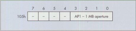
Figure 7. Contents of XGA POS Register 5: 1 MB Aperture
POS Register 5
The XGA Display Adapter also has a l MB aperture (not the same as the 4MB
aperture just mentioned) through which the video memory also can be accessed.
As shown in Figure 7, bits 0 through 3 of XGA POS Register 5 define where the I
MB aperture is located in the system address space.
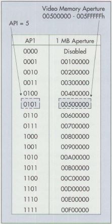
Figure 8. Video Memory 1 MB Aperture Base Address
Figure 8 shows the correspondence between the contents of the four-bit field
labeled AP1 in Figure 7 and the address of the 1MB aperture. In Figure 8, when
the four bits in AP1 are set to 5 (0101b), the video buffer can be accessed
through the 1 MB aperture located between addresses 00500000h and
005FFFFFh.
Jim Paolantonio is an advisory engineer in visual subsystems
within the IBM Entry Systems Technology laboratory in Boca Raton, Florida. His
current responsibilities include Very Large-Scale Integration (VLSI)
Liquid-Crystal Display (LCD) controller-chip development for portable systems.
Jim's previous assignment was XGA video hardware development for the IBM PS/2
Model 90 XP 486. He has also been a member of development engineering teams for
the IBM PS/2 Model 80, PC AT®, and PCIXT™. Jim holds BS and MS degrees in
electrical engineering from Purdue University.
|