|
184-028 IBM Portable PC 5155 Model 68
5155 Planar
SW1 System DIP Switch
640K Hack
Planar Memory Error Codes
5155 Origins
5155 Planar
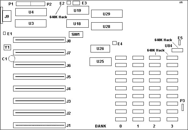
C1 Trimmer capacitor
E1 Pads for 2-pin header
E2 Pads for 4-pin header
E3 Pads for 8-pin header
E4 Pads for 4-pin header
E5 Pads for 3-pin header
J1-8 8-bit ISA slots
P1,2 Power Connector
P3 Speaker
SW1 System DIP Switch
U3 8088
U4 Socket for 8087
|
U18 MK38036N-25
U19 AM9265DPC34567
U25 8295A
U26 8253-5
U28 8237A-5 BIOS/Basic
U29 8255A-5 ROM
U30-38
U46-54
U59-67
U75-83
U84 empty 16-pin DIP socket
Y1 14.318 xtal
|
SW1 System DIP Switch
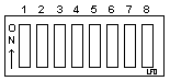
1 POST Mode
  ON       Continuous loop for diagnostic use
  OFF      Normal Operation
2 Math Coprocessor
  ON       8087 Not Installed
  OFF      8087 Installed (Seems wrong, but...)
3,4 Planar Memory
  ON/ON    1 Bank  (64K)
  OFF/ON   2 Banks (128K)
  ON/OFF   3 Banks (192K)
  OFF/OFF  4 Banks (256k)
5,6 Display Attached
  ON/ON    EGA,VGA
  OFF/ON   CGA (40x25 Color)
  ON/OFF   CGA (80x25 Color)
  OFF/OFF  Monochrome
7,8 Diskette
  ON/ON    1 Floppy Installed
  OFF/ON   2 Floppies Installed
  ON/OFF   3 Floppies Installed
  OFF/OFF  4 Floppies Installed
640K Hack
Gfretwell wrote:
The XT supports 640k and with the addition of one chip 74LS158
in u84 (plug in) and a jumper it will support 640kb on the system board
with 2 banks of 256 chips and 2 banks of 64s. Weee! It was still a handy
trick for saving slots. You can also plug in a 5162 (286) board with no
modifications. A handy 5155 "luggable" trick
Bob Eager says:
> Which jumper?
Looking from the front, about halfway back on the right edge of the
planar. There are two sets of pads, and the pair you need should be labeled
pads 1 and 2 on E2. Jumper those, either with a wire bridge or a proper
jumper block.
Then put a 74LS158 into the empty socket near front center (U84) and
replace memory banks 2 and 3 (which normally take 4164 (64K chips)) with
41256-15 chips. Make sure switches 3 and 4 are OFF on DIP switch bank SW1.
Access is a problem as the FDD bracket gets in the way of both operations.
Since I wanted to put a removable jumper block at E2 (so I could back out
the mod. if necessary) I just took the entire planar out!
> What did the reset switch attach to?
Ground and one of the pins on the 8284 clock/reset chip
(rear, near right hand side looking from front, near the keyboard socket).
Probably should have used a resistor but didn't. The chip is socketed so
I used solid core, thin wire, removed chip from socket, poked wires into
socket and put the chip back! Pin 9 is ground, and pin 11 is reset input
(active low).
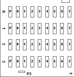
5155 Planar Memory Error Codes
|
Memory failures are displayed as a 7 character code followed by a 201.
If the first digit is 0, 1, 2, 3 then it's a planar memory failure.0,1,2,3
indicates the bank with the memory failure. Digits 6 and 7 show the failing
module.
Sixth and seventh characters
00  01  02  04  08  10  20  40  80
P   0   1   2   3   4   5   6   7

Example - 3C000 40 201
            |    |  |
Bank 3 -----|    |  |---- Memory Failure
                 |
            Failing Bit
|
5155 Origins
Rick Ekblaw wrote:
The 5155, called the PC Portable by IBM but usually called
the "Luggable" by everyone else, was basically a PC/XT with a small, built-in
amber composite monitor (driven by a standard CGA adapter), so you could
use the PC/XT Advanced Diagnostics on it. Lots of folks put a half-high
hard drive in it instead of a second floppy drive, the Seagate ST-225 was
commonly used for the task (or the ST-238R if you opted for an RLL hard
drive controller). The 5155 power supply provided only 114 watts instead of
the 5160's 130 watt supply, so you didn't want the hard drive drawing too much
power.
|