|
Pinouts:
8-bit Section
16-bit Section
32-bit Section
Matched-Memory Extension (MME)
Auxiliary Video Extension (AVE)
Base Video Extension (BVE)
Signal Descriptions:
Micro Channel Buses and Signals
Arbitration Bus and Associated Signals
Address Bus and Associated Signals
Data Bus and Associated Signals
Interrupt Signals
Other Micro Channel Signals
Channel Signal Groups (Digital)
Matched-Memory Extension Signal Descriptions
Auxiliary Video Extension Signal Descriptions
Micro Channel Architecture Base and Extensions
All drawings created by Tomáš Slavotínek.
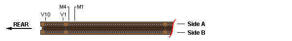
Notes:
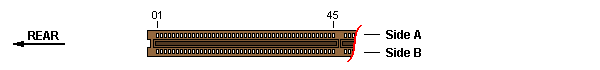
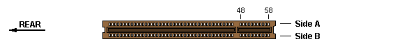
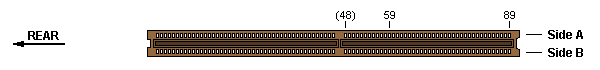
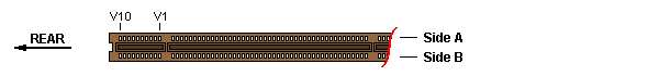
The "component side" (A) and "solder side" (B) refers to an installed adapter card.
The "Rear" arrow points towards the back side of the planar/system unit.
The physical key between pins 45 and 48 serves as a reference point for all connector types.
8-bit Section
| Pin | Signal | | Pin | Signal |
|---|
| B01 | AUDIO GND | A01 | -CD SETUP |
| B02 | AUDIO | A02 | MADE 24 |
| B03 | GND | A03 | GND |
| B04 | 14.3 MHz OSC | A04 | A 11 |
| B05 | GND | A05 | A 10 |
| B06 | A 23 | A06 | A 09 |
| B07 | A 22 | A07 | +5 Vdc |
| B08 | A 21 | A08 | A 08 |
| B09 | GND | A09 | A 07 |
| B10 | A 20 | A10 | A 06 |
| B11 | A 19 | A11 | +5 Vdc |
| B12 | A 18 | A12 | A 05 |
| B13 | GND | A13 | A 04 |
| B14 | A 17 | A14 | A 03 |
| B15 | A 16 | A15 | +5 Vdc |
| B16 | A 15 | A16 | A 02 |
| B17 | GND | A17 | A 01 |
| B18 | A 14 | A18 | A 00 |
| B19 | A 13 | A19 | +12 Vdc |
| B20 | A 12 | A20 | -ADL |
| B21 | GND | A21 | -PREEMPT |
| B22 | -IRQ 09 | A22 | -BURST |
| B23 | -IRQ 03 | A23 | -12 Vdc |
| B24 | -IRQ 04 | A24 | ARB 00 |
| B25 | GND | A25 | ARB 01 |
| B26 | -IRQ 05 | A26 | ARB 02 |
| B27 | -IRQ 06 | A27 | -12 Vdc |
| B28 | -IRQ 07 | A28 | ARB 03 |
| B29 | GND | A29 | ARB/-GNT |
| B30 | -DPAREN 1) | A30 | -TC |
| B31 | DPAR(0) 1) | A31 | +5 Vdc |
| B32 | -CHCK | A32 | -S0 |
| B33 | GND | A33 | -S1 |
| B34 | -CMD | A34 | M/-IO |
| B35 | CHRDYRTN | A35 | +12 Vdc |
| B36 | -CD SFDBK | A36 | CD CHRDY |
| B37 | GND | A37 | D 00 |
| B38 | D 01 | A38 | D 02 |
| B39 | D 03 | A39 | +5 Vdc |
| B40 | D 04 | A40 | D 05 |
| B41 | GND | A41 | D 06 |
| B42 | CHRESET | A42 | D 07 |
| B43 | -SD STROBE 1) | A43 | GND |
| B44 | -SDR(0) 1) | A44 | -DS 16 RTN |
| B45 | GND | A45 | -REFRESH |
| B46 | PHYSICAL KEY | A46 | PHYSICAL KEY |
Notes:
- Optional signal. The corresponding pin was marked as "Reserved" in the earlier specifications.
16-bit Section
| Pin | Signal | | Pin | Signal |
|---|
| B47 | PHYSICAL KEY | A47 | PHYSICAL KEY |
| B48 | D 08 | A48 | +5 Vdc |
| B49 | D 09 | A49 | D 10 |
| B50 | GND | A50 | D 11 |
| B51 | D 12 | A51 | D 13 |
| B52 | D 14 | A52 | +12 Vdc |
| B53 | D 15 | A53 | DPAR(1) 1) |
| B54 | GND | A54 | -SBHE |
| B55 | -IRQ 10 | A55 | -CD DS 16 |
| B56 | -IRQ 11 | A56 | +5 Vdc |
| B57 | -IRQ 12 | A57 | -IRQ 14 |
| B58 | GND | A58 | -IRQ 15 |
Notes:
- Optional signal. The corresponding pin was marked as "Reserved" in the earlier specifications.
32-bit Section
| Pin | Signal | | Pin | Signal |
|---|
| B59 | Reserved 2) | A59 | Reserved 2) |
| B60 | Reserved 2) | A60 | Reserved 2) |
| B61 | -SDR(1) 1) | A61 | GND |
| B62 | -MSDR 1) | A62 | Reserved |
| B63 | GND | A63 | Reserved |
| B64 | D 16 | A64 | -SFDBKRTN 1) |
| B65 | D 17 | A65 | +12 Vdc |
| B66 | D 18 | A66 | D 19 |
| B67 | GND | A67 | D 20 |
| B68 | D 22 | A68 | D 21 |
| B69 | D 23 | A69 | +5 Vdc |
| B70 | DPAR(2) 1) | A70 | D 24 |
| B71 | GND | A71 | D 25 |
| B72 | D 27 | A72 | D 26 |
| B73 | D 28 | A73 | +5 Vdc |
| B74 | D 29 | A74 | D 30 |
| B75 | GND | A75 | D 31 |
| B76 | -BE 0 | A76 | DPAR(3) 1) |
| B77 | -BE 1 | A77 | +12 Vdc |
| B78 | -BE 2 | A78 | -BE 3 |
| B79 | GND | A79 | -DS 32 RTN |
| B80 | TR 32 | A80 | -CD DS 32 |
| B81 | A 24 | A81 | +5 Vdc 3) |
| B82 | A 25 | A82 | A 26 |
| B83 | GND | A83 | A 27 |
| B84 | A 29 | A84 | A 28 |
| B85 | A 30 | A85 | +5 Vdc |
| B86 | A 31 | A86 | -APAREN 1) |
| B87 | GND | A87 | APAR(0) 1) |
| B88 | APAR(2) 1) | A88 | APAR(1) 1) |
| B89 | APAR(3) 1) | A89 | GND |
Notes:
- Optional signal. The corresponding pin was marked as "Reserved" in the earlier specifications.
- This is where the 16-bit slot physically ends. Universal 16/32-bit cards will have a cutout in place of these pins. Cards designed exclusively for the 32-bit slot don't have this cutout.
- This pin was incorrectly marked as +12 Vdc in some early documentation.
Matched-Memory Extension (MME)

| Pin | Signal | | Pin | Signal |
|---|
| BM4 | GND | AM4 | Reserved |
| BM3 | Reserved | AM3 | -MMC CMD |
| BM2 | -MMCR | AM2 | GND |
| BM1 | Reserved | AM1 | -MMC |
Auxiliary Video Extension (AVE)
| Pin | Signal | | Pin | Signal |
|---|
| BV10 | ESYNC | AV10 | VSYNC |
| BV9 | GND | AV9 | HSYNC |
| BV8 | P5 | AV8 | BLANK |
| BV7 | P4 | AV7 | GND |
| BV6 | P3 | AV6 | P6 |
| BV5 | GND | AV5 | EDCLK |
| BV4 | P2 | AV4 | DCLK |
| BV3 | P1 | AV3 | GND |
| BV2 | P0 | AV2 | P7 |
| BV1 | GND | AV1 | EVIDEO |
Base Video Extension (BVE)
| Pin | Signal | | Pin | Signal |
|---|
| BV10 | ESYNC | AV10 | VSYNC |
| BV9 | GND | AV9 | HSYNC |
| BV8 | P5 | AV8 | BLANK |
| BV7 | P4 | AV7 | GND |
| BV6 | P3 | AV6 | P6 |
| BV5 | GND | AV5 | EDCLK |
| BV4 | P2 | AV4 | DCLK |
| BV3 | P1 | AV3 | GND |
| BV2 | P0 | AV2 | P7 |
| BV1 | GND | AV1 | EVIDEO |
| — | PHYSICAL KEY | — | PHYSICAL KEY |
| — | PHYSICAL KEY | — | PHYSICAL KEY |
| BM4 | GND | AM4 | Reserved |
| BM3 | Reserved | AM3 | -MMC CMD |
| BM2 | -MMCR | AM2 | GND |
| BM1 | Reserved | AM1 | -MMC |
Micro Channel Buses and Signals
The Micro Channel architecture consists of:
- An arbitration bus and associated signals
- An address bus and associated signals
- A data bus and associated signals
- Interrupt signals
- Other Micro Channel signals
- Optional extensions for:
- Matched memory extension signals
- Video extension signals
Throughout this page, a minus sign (-) in front of a signal name indicates
that the signal is active when it is at a low-voltage level. When no minus sign
appears, the signal is active when it is at a high-voltage level. For example,
-CMD specifies the signal is active low. Also, ARB/-GNT is in the ARB state
when it is at a high level and is in the -GNT state when it is at a low
level.
All of the logic signal lines are transistor-transistor logic (TTL)
compatible.
Reserved: Any signals shown or described as "Reserved" should not be
driven or received. These signals are reserved to allow compatibility with
future implementations of the channel interface. Serious compatibility
problems, loss of data, or permanent damage can result to features or the
system if these signals are misused.
Note: Adapter designs should not extend the
card-edge connector beyond the basic 16- or 32-bit connector unless the signals
provided by the extension are used by the adapter. Adapters for the Micro
Channel architecture have special design criteria. See
"Micro Channel Adapter Design." (PDF)
Arbitration Bus and Associated Signals
The arbitration bus and associated signals allow arbitrating
participants (the system master, bus masters, and DMA slaves) to
request and gain ownership of the channel. The resolution of
multiple arbitration requests results in granting ownership of the
channel to the highest-priority requester. See
"Arbitration" (PDF) for more
information.
ARB0 — ARB3: Arbitration Bus: These signals make up the
arbitration bus. They are driven by the system master, bus masters, and DMA
slaves to present their arbitration level when requesting ownership of the
channel. ARB0 (least-significant) through ARB3 (most-significant) support up to
16 arbitration levels.
The highest value of the arbitration bus (hex F) has the lowest priority,
and the lowest value (hex 0) has the highest priority. To participate in the
arbitration procedure, an arbitrating participant must present its arbitration
level immediately after the rising edge of ARB/-GNT. All arbitrating
participants monitor the arbitration bus, and those with lower priority
arbitration levels withdraw them by not driving less-significant arbitration
bits.
The arbitration level of the highest-priority requester is valid on the
arbitration bus after a settling time. After the channel is granted to the
highest-priority requester, that requester continues to drive its arbitration
level on the bus.
ARB/-GNT: Arbitrate/-Grant: Only the central arbitration control
point drives this signal. The negative-to-positive transition of ARB/-GNT
initiates an arbitration cycle. When in the ARB state, this signal indicates an
arbitration cycle is in progress. When in the -GNT state, this signal indicates
the acknowledgment from the central arbitration control point to the
arbitrating participants and the DMA controller that channel ownership has been
granted. This signal is driven to the ARB state by the central arbitration
control point following the end of transfer (EOT). See
"Central Arbitration Control
Point" (PDF) for a description of the end of transfer.
Note: The system master can perform data transfers
during arbitration (ARB/-GNT in the ARB state).
-BURST: -Burst: This signal is optionally driven by the winning
arbitrating participant or the DMA controller after ARB/-GNT is driven to the
-GNT state. This signal indicates to the central arbitration control point that
the controlling master will use the channel for one or more consecutive data
transfer cycles. This type of data transfer is called burst transfer.
-PREEMPT: -Preempt: This signal is used by arbitrating participants
to request use of the channel through arbitration. Any arbitrating participant
that requires ownership of the channel drives -PREEMPT active, causing an
arbitration cycle to occur. When a participant is granted control of the
channel, it stops driving -PREEMPT. All arbitrating participants that have not
been granted ownership keep their requests pending by continuing to drive
-PREEMPT active. All masters and DMA slaves that use burst transfer must
receive -PREEMPT.
Address Bus and Associated Signals
The address bus and the associated signals are used by the controlling
master to assert the memory address or the I/O address (M/-IO), to enable a
slave to latch the address and status signals (-S0, -S1), and to indicate that
the memory address is greater than 16 MB.
A0 — A23: Address Bits 0 through 23: These lines, along with
A24 through A31, make up the address bus. These lines are driven by the
controlling master to address memory, I/O slaves, and, optionally, DMA slaves,
A0 is the least-significant bit and A23 is the most-significant bit. These 24
address lines allow access of up to 16 MB of memory. Only the lower 16 address
lines (A0 through A15) are for I/O operations, and all 16 lines must be decoded
by the I/O slave. A0 through A23 are generated by the controlling master. Valid
addresses, generated by the controlling master, are unlatched on the channel
and, if required, must be latched by the slaves using either the leading or
trailing edge of -ADL or the leading edge of -CMD.
A24 — A31: Address Bits 24 through 31: These lines, along with
A0 through A23 are driven by the controlling master to address memory attached
to the channel. A0 is the least-significant bit and A31 is the most-significant
bit. These additional address lines allow access of up to 4 GB of memory. A24
through A31 are generated by the controlling master. Valid addresses, generated
by the controlling master, are unlatched on the channel and, if required, must
be latched by the slaves using either the leading or trailing edge of -ADL or
the leading edge of -CMD.
Note: A0-A31 are used to transfer data during a
64-bit streaming data cycle.
-ADL: -Address Decode Latch: This signal, driven by the controlling
master, is provided as a convenient way for the slave to latch valid address
decodes and status bits.
-APAREN: -Address Parity Enable: This optional signal is driven
active by a master when the master places an address on the bus. This signal
indicates to a slave that the address parity signals are valid.
APAR0 — APAR3: Address Parity Bits 0 through 3: These optional
signals are driven by a master when an address is placed on the address bus.
These signals represent the odd parity of the address bits on the address bus
during both read and write operations. (Odd parity is the condition where the
total number of 1s in a byte of data, including the parity bit, is odd.)
APAR(0) represents the odd parity of A(0-7)
APAR(1) represents the odd parity of A(8-15)
APAR(2) represents the odd parity of A(16-23)
APAR(3) represents the odd parity of A(24-31)
During both read and write operations, a master generates a parity bit for
each valid address byte, and the receiving slave optionally performs the parity
checking to ensure the integrity of the address.
Note: APAR0 - APAR3 represent data parity during
64-bit streaming data cycle when -DPAREN is active.
APAR(0) represents the odd parity of D(32-39)
APAR(1) represents the odd parity of D(40-47)
APAR(2) represents the odd parity of D(48-55)
APAR(3) represents the odd parity of D(56-63)
-CD SFDBK (n): -Card Selected Feedback: This signal is driven active
by the selected slave as a positive acknowledgement of the slave's selection.
The (n) indicates this signal is unique to each channel connector (one
independent signal per connector). This signal is unlatched and driven by the
selected slave. The slave does not drive -CD SFDBK during the configuration
procedure (-CD SETUP active).
Note: Memory that contains diagnostic code must
not drive -CD SFDBK during the diagnostic operation.
MADE 24: Memory Address Enable 24: This signal is driven by the
controlling master and decoded by all memory slaves, regardless of the size of
their address-space. When this signal is active, A24 - 31 are undefined.
- A master driving only A0 - A23 drives MADE 24 active
- A master driving A0 - A31 drives MADE 24:
- Active when all bits in A24 - A31 are 0
- Inactive when any bit in A24 - A31 is 1
M/-IO: Memory/-Input Output: This signal is driven by the controlling
master and decoded by all slaves. This signal selects a memory cycle or an I/O
cycle. When this signal is in the M state, a memory cycle is selected. When
this signal is in the -IO state, an I/O cycle is selected.
-SFDBKRTN: Selected Feedback Return: This optional signal is
generated by the system logic from the AND of the -CD SFDBK(n) signals being
driven by slaves. This signal is a positive acknowledgement to the master from
the slave that the slave is at the address specified by the master. Masters
that support address parity must receive this signal.
Data Bus and Associated Signals
The data bus is used to transfer either 8, 16, 24, or 32 bits of data. The
associated signals indicate the amount of data transferred by the master in a
single transfer cycle, the size of the slave's data port, and the type (read or
write) of the data transfer.
D0 — D15: Data Bits 0 through 15: These lines, along with D16 -
D31, make up the data bus. The data bus is driven by any master or slave that
is transferring data. These lines (D0 - D15) provide data bits 0 through 15. D0
is the least-significant bit; D15 is the most-significant bit. The 16-bit
transfers from the controlling master to an 8-bit slave are converted by the
controlling master to two 8-bit transfers, and are transmitted on lines D0
through D7. An 8-bit slave must use D0 through D7 to communicate with the
controlling master.
D16 — D31: Data Bits 16 through 31: These lines, along with D0
- D15, make up the data bus. The data bus is driven by any master or slave that
is transferring data. These lines (D16 - D31) provide data bits 16 through 31.
D0 is the least-significant bit; D31 is the most-significant bit. The 32-bit
transfers from the controlling master to an 8-bit slave are converted to four
8-bit transfers by the controlling master, and are transmitted on lines D0
through D7. The 32-bit transfers from the controlling master to a 16-bit slave
are converted to two 16-bit transfers by the controlling master, and are
transmitted on lines D0 through D15.
-BE0 — -BE3: -Byte Enable 0 through 3: These signals are used
during data transfers with 32-bit slaves to indicate which data bytes are valid
on the data bus. Data transfers of 8, 16, 24, or 32 contiguous bits are
controlled by -BE0 through -BE3 during transfers involving 32-bit slaves only.
These signals are driven by the controlling master when TR 32 is inactive, and
by the central translator logic (for those operations involving a 16-bit master
with a 32-bit slave) when TR 32 is active. These signals are not latched on the
bus and, if required, are latched by 32-bit slaves. See
"Channel Support" (PDF) for
additional information.
-CD DS 16 (n): -Card Data Size 16: This signal is driven by 16-bit
and 32-bit slaves to indicate a 16-bit or 32-bit data port at the location
addressed. The (n) indicates this signal is unique to each channel connector
(one independent signal per connector). This signal is derived from a valid
unlatched address decode. -CD DS 16 is not driven by 8-bit slaves and is
inactive for an 8-bit data port.
-CD DS 32 (n): -Card Data Size 32: This signal, along with -CD DS 16,
is driven by 32-bit slaves to indicate a 32-bit data port at the location
addressed. The (n) indicates this signal is unique to a channel connector
position (one independent signal per connector). -CD DS 32 is derived from a
valid unlatched address decode. -CD DS 32 is inactive for an 8- or 16-bit data
port.
CD CHRDY (n): Channel Ready: This signal is normally active (ready)
and is driven inactive (not ready) by a slave to allow additional time to
complete a channel cycle. The (n) indicates this signal is unique to each
channel connector (one independent signal per connector).
During a read cycle, a slave ensures that data is valid within the time
specified after releasing the signal to a ready state. The slave also holds the
data long enough for the controlling master to sample the data. A slave can
also use this signal during a write cycle if more time is needed to store the
data. This signal is initially driven from a valid unlatched address decode and
status active.
CHRDYRTN: Channel Ready Return: This signal is the AND of CD CHRDY
(n). It is driven by the system logic. If all slaves drive CD CHRDY active,
this signal is active. CHRDYRTN allows the controlling master to monitor the
ready information.
-CMD: -Command: This signal is driven by the controlling master and
is used to define when data on the data bus is valid. The trailing edge of this
signal indicates the end of the bus cycle. This signal indicates to the slave
how long data is valid. During write cycles, the data is valid as long as -CMD
is active. During read cycles, the data is valid after the leading edge, but
before the trailing edge, of -CMD and is held on the bus until after -CMD goes
inactive. Slaves can latch address and status information with the leading edge
of -CMD.
-DPAREN: -Data Parity Enable: This optional signal is driven active
by the participant when data is placed on the data bus. This signal indicates
that the data parity signals are valid.
Note: APAR(0) - APAR(3) represent data parity
during 64-bit streaming data cycles when -DPAREN is active.
DPAR0 — DPAR1: Data Parity Bits 0 and 1: These optional signals
are driven by the participant when data is placed on the data bus. These
signals represent the odd parity of the data bits on the data bus during both
read and write operations. (Odd parity is the condition where the total number
of 1s in a byte of data, including the parity bit, is odd.)
DPAR(0) represents the odd parity of D(0-7).
DPAR(1) represents the odd parity of D(8-15).
During write operations, a master generates a parity bit for each data byte
being transferred, and the receiving slave optionally performs the parity
checking to ensure the integrity of the data. During read operations, a slave
generates a parity bit for each valid data byte, and the receiving master
performs the parity checking to ensure the integrity of the data.
DPAR2 — DPAR3: Data Parity Bits 2 and 3: These optional signals
are driven by the participant when data is placed on the data bus. These
signals represent the odd parity of the data bits on the data bus during both
read and write operations.
DPAR(2) represents the odd parity of D(16-23).
DPAR(3) represents the odd parity of D(24-31).
During write operations, a master generates a parity bit for each data byte
being transferred, and the receiving slave optionally performs the parity
checking to ensure the integrity of the data. During read operations, a slave
generates a parity bit for each valid data byte, and the receiving master
performs the parity checking to ensure the integrity of the data.
-DS 16 RTN: -Data Size 16 Return: This signal is driven by the system
logic. This signal is the AND of -CD DS 16 (n) from each channel connector. If
any slave drives its -CD DS 16 active, this signal is active. This signal
allows the controlling master to monitor the information about the selected
slave's data port size (see Table 1).
-DS 32 RTN: -Data Size 32 Return: This signal is driven by the system
logic. This signal is the AND of -CD DS 32 (n) from each channel connector. If
any slave drives its -CD DS 32 active, this signal is active. This signal
allows the controlling master to monitor the information about the selected
slave's data port size.
-DS 16
RTN | -DS 32
RTN | Data Port Size |
|---|
| 1 | 1 | 8-Bit Data Port |
| 1 | 0 | Not Valid |
| 0 | 1 | 16-Bit Data Port |
| 0 | 0 | 32-Bit Data Port |
Table 1. Port Size of Selected Slave
-MSDR: -Multiplexed Streaming Data Request: This signal is driven by
a slave to indicate to the controlling master that the slave is capable of
64-bit streaming data transfers.
-SBHE: -System Byte High Enable: This signal is driven by the
controlling master to indicate and enable transfers of data on D8 - D15. It is
used with A0 to distinguish between high-byte transfers (D8 — D15) and
low-byte transfers (D0 — 7) and double-byte (16-bit) transfers to 16-bit
data ports. All 16-bit slaves receive this signal.
-SD STROBE: -Streaming Data Strobe: The controlling master and the
slave use this signal to clock data on and off the data bus. This optional
signal is driven by the controlling master. This signal also indicates to the
slave that the controlling master supports streaming data.
-SDR(0): -Streaming Data Request 0: This optional signal is driven by
a slave to indicate to the controlling master that the slave is capable of
streaming data, and also indicates the maximum clocking rate the slave
supports.
-SDR(1): -Streaming Data Request 1: This optional signal is driven by
a slave to indicate to the controlling master that the slave is capable of
streaming data, and also indicates the maximum clocking rate the slave
supports.
| -SDR | Decoded Streaming Rate |
|---|
| 0 | 1 |
|---|
| 1 | 1 | Basic Transfer Cycle (200 ns) |
| 0 | 1 | Streaming Data Procedure (100 ns) |
| 1 | 0 | Reserved / "16 MHz" Streaming Data Procedure (62.5 ns) ** |
| 0 | 0 | Enhanced Streaming Data Procedure (50 ns) * |
Table 2. Streaming Data Rates
(* Late systems only, ** Possibly never implemented,
see US5109490 & IPCOM000106659)
-S0, -S1: -Status 0, -Status 1: These status signals are driven by
the controlling master to indicate the start of a data transfer cycle and also
define the type of data transfer. When used with M/-IO, memory read or write
cycles are distinguished from I/O read or write cycles. These signals are
latched by the slave, as required, using the leading edge of -CMD, or the
leading or trailing edge of -ADL.
Data is transferred to or from the data bus based on -CMD and a latched
decode of the address, the status lines (-S0 exclusive-OR -S1), and M/-IO.
Slaves must support a full decode of -S0 and -S1. The following table shows
the states of M/-IO, -S0, and -S1 in decoding I/O and memory read and write
commands.
M/
-IO | -S0 | -S1 | Function |
|---|
| 0 | 0 | 0 | Reserved |
| 0 | 0 | 1 | I/O Write Command |
| 0 | 1 | 0 | I/O Read Command |
| 0 | 1 | 1 | Inactive |
| 1 | 0 | 0 | Reserved |
| 1 | 0 | 1 | Memory Write Command |
| 1 | 1 | 0 | Memory Read Command |
| 1 | 1 | 1 | Inactive |
Table 3. I/O and Memory Transfer Controls
An I/O write command instructs an I/O slave to receive the data from the
data bus. An I/O read command instructs an I/O slave to drive its data onto the
data bus.
A memory write command instructs a memory slave to receive the data from the
data bus. A memory read command instructs a memory slave to drive its data onto
the data bus.
-TC: -Terminal Count: This signal is driven by the DMA controller and
provides a pulse during a read or write command to the DMA slave to indicate
that the terminal count of the current DMA channel has been reached. This
indicates to the DMA slave that this is the last cycle to be performed. -TC is
driven active on the channel during DMA operations only.
TR 32: Translate 32: This signal is driven inactive by 32-bit
controlling masters and received by the central translator logic. The signal
indicates to the central translator logic that the controlling master is
performing data steering. TR 32 can also be received by any 32-bit slave. See
"Data Steering" (PDF) for
information about the central translator logic.
Interrupt Signals
-IRQ 3—7, -IRQ 9—12, and -IRQ 14—15: -Interrupt
Request: An interrupt request is generated when an I/O slave drives one of the
'interrupt request' signals low. These signals make up the set of interrupt
signals. The polarity of these signals makes it possible for multiple slaves to
concurrently share the same interrupt level.
Other Micro Channel Signals
AUDIO: Audio Sum Node: This analog signal is the sum of all the audio
signals being driven. It is used to drive audio signals from an adapter to the
system audio output and between adapters. The frequency response of the audio
signal is 50 Hz to 10 kHz ± 3 dB. The maximum signal amplitude is 2.5
Vac peak-to-peak, at a dc offset of 0.0 Vdc ± 50 millivolts. The noise
level is limited to a maximum of 50 millivolts peak-to-peak.
AUDIO GND: Audio Ground: This is the analog ground return signal for
the audio subsystem.
-CD SETUP (n): -Card Setup: This signal is driven by system logic to
individually select channel connectors. The (n) indicates this signal is unique
to each channel connector (one independent signal per connector). When this
signal is activated, a specific channel connector is selected, and, if an
adapter is present, access is gained to configuration data at that connector.
The adapter ID and configuration data is obtained by an I/O read during a setup
cycle; the configuration data is stored by an I/O write during a setup
cycle.
-CHCK: -Channel Check: This signal is driven active by a slave to
report an exception condition, and optionally, it can be driven by a
master.
CHRESET: Channel Reset: This signal is generated by the system logic
to reset or initialize all adapters at power-on or when a low voltage condition
is detected. The system can also activate this signal under program
control.
OSC: Oscillator: This signal is a high-speed clock driven by the
system logic, with a frequency of 14.31818 MHz ± 0.01%. The high-level
pulse width (more than 2.3 Vdc) and the low-level pulse width (less than 0.8
Vdc) must not be less than 20 nanoseconds each.
-REFRESH: -Refresh: This signal is driven by the system logic and is
used to indicate that a memory refresh operation is in progress. Memory slaves
that do not need to perform refresh operations do not need to receive this
signal.
Channel Signal Groups (Digital)
The following figure lists the digital Micro Channel signals and shows
what type of driver or receiver is required. The 'audio' and 'audio
ground' signals are analog signals. For further information about
these signals, see "Other Micro
Channel Signals." (PDF)
When a Micro Channel adapter combines the functions of bus masters and
slaves, the signals driven and received by the adapter are a superset of the
selected functions.
For example:
- An adapter that combines a slave function with a bus master function must
drive and receive all signals required by a slave and all signals required by a
bus master.
- An adapter that combines an I/O slave function with a memory slave or DMA
slave function, must drive and receive all signals required by both
slaves.
Note: All adapters must support setup.
The central arbitration control point, central steering logic, and central
translator logic are packaged within the system logic. The system logic also
includes circuitry for memory refresh, the oscillator, and channel reset.
The signals for the 16-bit adapter are a subset of the signals for the
32-bit adapter.
| Signal Name | System
Master | DMA
Cntlr | Bus
Master | DMA
Slave | Memory
Slave | I/O
Slave | Driver
Type |
|---|
| D/R | D/R | D/R | D/R | D/R | D/R | Signal
Group |
| A(0-15) | D/- | D/- | D/- | -/O | -/R | -/R | TS (1) |
| A(16-23) | D/- | D/- | D/- | -/- | -/R | -/- | TS (1) |
| A(24-31) | */- | */- | */- | -/- | -/* | -/- | TS (1) |
| -ADL | D/- | D/- | D/- | -/O | -/O | -/O | TS (1) |
| APAR(0-3) | O/- | O/- | O/- | -/O | -/O | -/O | TS (2) |
| -APAREN | O/- | O/- | O/- | -/O | -/O | -/O | TS (2) |
| ARB(0-3) | O/O | -/R | D/R | D/R | -/- | -/- | OC (5) |
| ARB/-GNT | D/- | -/R | -/R | -/R | -/- | -/- | BD (4) |
| -BE(0-3) | */- | */- | */- | -/* | -/* | -/* | TS (1) |
| -BURST | O/R | D/R | O/- | O/- | -/O | -/O | OC (5) |
| CD CHRDY (n) | -/R | -/- | -/- | O/- | O/- | O/- | TP (3) |
| -CD DS 16 (n) | -/R | -/- | -/- | $/- | $/- | $/- | TP (3) |
| -CD DS 32 (n) | -/* | -/- | -/- | */- | */- | */- | TP (3) |
| -CD SETUP (n) | D/- | -/@ | -/@ | -/@ | -/@ | -/@ | TP (8) |
| -CD SFDBK (n) | -/R | -/- | -/- | D/- | D/- | D/- | TP (3) |
| -CHCK | -/R | O/R | O/R | O/- | O/- | O/- | OC (6) |
| CHRDYRTN | D/- | -/R | -/R | -/- | -/- | -/- | BD (4) |
| CHRESET | D/- | -/R | -/R | -/R | -/R | -/R | BD (4) |
| -CMD | D/- | D/- | D/- | -/R | -/R | -/R | TS (1) |
| D(0-7) | D/R | D/R | D/R | D/R | D/R | D/R | TS (2) |
| D(8-15) | D/R | D/R | D/R | $/$ | $/$ | $/$ | TS (2) |
| D(16-31) | */* | */* | */* | */* | */* | */* | TS (2) |
| DPAR(0) | O/O | O/O | O/O | O/O | O/O | O/O | TS (2) |
| DPAR(1) | O/O | O/O | O/O | O/O | O/O | O/O | TS (2) |
| DPAR(2-3) | O/O | O/O | O/O | O/O | O/O | O/O | TS (2) |
| -DPAREN | O/O | O/O | O/O | O/O | O/O | O/O | TS (2) |
| -DS 16 RTN | D/- | -/R | -/R | -/- | -/- | -/- | BD (4) |
| -DS 32 RTN | */- | -/* | -/* | -/- | -/- | -/- | BD (4) |
| -IRQ (N) | O/R | O/- | O/O | O/- | O/- | O/- | OC (6) |
| M/-IO | D/- | D/- | D/- | -/R | -/R | -/R | TS (1) |
| MADE 24 | D/- | D/- | D/- | -/- | -/R | -/- | TS (1) |
| -MSDR | -/O | -/O | -/O | O/- | O/- | O/- | TS (1) |
| OSC | D/- | -/O | -/O | -/O | -/O | -/O | CD (7) |
| -PREEMPT | D/R | -/- | D/O | D/O | -/- | -/- | OC (5) |
| -REFRESH | D/- | -/- | -/- | -/- | -/O | -/- | TS (1) |
| -S0,-S1 | D/* | D/- | D/- | -/R | -/R | -/R | TS (1) |
| -SBHE | D/* | D/- | D/- | -/# | -/# | -/# | TS (1) |
| -SFDBKRTN | O/- | -/O | -/O | -/- | -/- | -/- | BD (4) |
| -SD STROBE | O/- | O/- | O/- | -/O | -/O | -/O | TS (1) |
| -SDR(0) | -/O | -/O | -/O | O/- | O/- | O/- | TS (1) |
| -SDR(1) | -/O | -/O | -/O | O/- | O/- | O/- | TS (1) |
| -TC | -/- | D/- | -/- | -/R | -/- | -/- | TS (1) |
| TR 32 | */R | */- | */- | -/O | -/O | -/O | TS (1) |
Table 4. Driver and Receiver Requirements and Options
Legend:
D = Drive Enabled
R = Receive Enabled
O = Optional
# = Required for 16-bit devices
$ = Required for 16- or 32-bit devices
* = Required for 32-bit devices
- = Not Implemented
@ = -CD SETUP is received by all adapters
OC = Open Collector
TS = Tri-State
TP = Totem Pole
BD = Bus Driver
CD = Clock Driver
N = IRQ(9-12,14,15,3-7)
Matched-Memory Extension Signal Descriptions
The matched-memory extension can, in some cases, improve the data transfer
capabilities between the system master and channel-resident memory. The
matched-memory signal-sequence and signal-timing specifications are system
dependent. For more information, see the technical manuals for the systems that
support the matched-memory signals.
-MMC: -Matched Memory Cycle: This signal is driven by the system
logic to indicate to the channel slaves that the system microprocessor is the
controlling master and is able to run a matched-memory cycle.
-MMCR: -Matched Memory Cycle Request: This is a bus cycle
control-input signal. -MMCR is driven by a 16- or 32-bit channel slave to
request the faster cycle available on the system bus.
-MMC CMD: -Matched Memory Cycle Command: This output signal to the
bus is generated for system microprocessor bus cycles only.
-MMC CMD defines when data is valid on the bus during a matched-memory
cycle.
Auxiliary Video Extension Signal Descriptions
The auxiliary video extension allows optional video adapters to share video
resources with the base video subsystem. The base video can be on the system
board or on an adapter with the base video extension. When the base video
subsystem is on the system board, support of the auxiliary video extension is
direct. When the base video subsystem is on an adapter, support of the
auxiliary video extension is through the base video extension. The signals and
signal timings for the auxiliary and base video extensions are system
dependent.
The following are signal descriptions for the auxiliary video extension
of the channel connector.
VSYNC: Vertical Synchronization: This signal is the vertical
synchronization signal to the display. See also the ESYNC description.
HSYNC: Horizontal Synchronization: This signal is the horizontal
synchronization signal to the display. See also the ESYNC description.
BLANK: Blanking Signal: This signal is connected to the BLANK input
of the video digital-to-analog converter (DAC). When active (0 Vdc),
this signal tells the DAC to drive its analog color outputs to 0 Vdc.
See also the ESYNC description.
P0 - P7: Palette Bits: These eight signals contain video information
and comprise the picture element (PEL) address inputs to the video
DAC. See also the EVIDEO description.
DCLK: Dot Clock: This signal is the PEL clock used by the DAC to
latch the digital video signals, P7 through P0. The signals are latched
into the DAC on the rising edge of DCLK.
This signal is driven through the EXTCLK input to the system board
video when DCLK is driven by the adapter. If an adapter is providing
the clock, it must also provide the video data to the DAC. See the
EDCLK description.
ESYNC: External Synchronization: This signal is the output-enable
signal for the buffer that drives BLANK, VSYNC, and HSYNC. ESYNC is tied
to +5 Vdc through a pull-up resistor.
ESYNC high - the system board video drives BLANK, VSYNC, and HSYNC
ESYNC low - the adapter drives BLANK, VSYNC, and HSYNC
EVIDEO: External Video: This signal is the output-enable signal for
the buffer that drives P7 through P0. EVIDEO is tied to +5 Vdc through a
pull-up resistor.
EVIDEO high - the system board video drives P7 through P0
EVIDEO low - the adapter drives P7 through P0
EDCLK: External Dot Clock: This signal is the output-enable signal
for the buffer that drives DCLK. EDCLK is tied to +5 Vdc through a
pull-up resistor.
EDCLK high - the system board video is the source of DCLK to the DAC and the adapter
Note: Miscellaneous Output register should not select clock source 2 (010 binary).
EDCLK low - the adapter drives DCLK (and must also provide video data to DAC)
Note: Miscellaneous Output register must select clock
source 2 (010 binary).
See "Video Subsystem" (PDF) and the
Auxiliary Video Extension page for
more information.
Micro Channel Architecture Base and Extensions
See "32-Bit Connector and
Extensions" (PDF) for the buses and signals available for use with the 32-bit
connector. The optional extensions signals are shown at the top of the figure
and the optional connector pins at the bottom of the figure.
See "16-Bit Connector and Extensions" (PDF) for the buses and signals available for use
with the 16-bit connector. The optional extensions signals are shown
at the top of the figure and the optional connector pins at the bottom
of the figure. The 16-bit connector is a subset of the 32-bit connector.
"Connector Definition" (PDF) contains
the physical specifications for the connectors.
|