Source: BYTE Magazine, September 1988 (link), Page 257+
Authors: Ron Peterson, Carrell R. Killebrew Jr., Tom Albers, and Karl Guttag
Ed.
More editing needs to be done due to the seeming original
editing mistakes that were caused / hidden by placing the
text in flowing columns. Also, having columns of text
above, to the side, or below illustrations just makes it
harder to keep continuity...
The new TMS34020 32-bit graphics
microprocessor (the '20) is well suited to workstations
and personal computers requiring highly interactive user
interfaces. The '20 is also suited to laser printers,
which are becoming more performance hungry, with
requirements for on-the-fly font compilation, and the
increased complexity of page-description languages, which
are constantly demanding more performance.
Data and image compression such as
facsimile and CD-ROM are other areas where the '20 will
find ready applications, since fast bit addressable
processors provide inherent advantages over
general-purpose processors for performing the Huffman-type
encoding and decoding necessary for CCITT Groups 3 and 4
fax standards. In fact, for TMS340 Graphics System
Processors (GSPs), fax-type compression and decompression
is just another program (i.e., no additional hardware is
required).
A Chip off the
Old Block
The '20 is the newest member of Texas
Instruments' (TI) TMS340 GSP family. Depending on the
instruction mix, it's between 6 and 50 times faster in key
graphics operations than its predecessor, the TMS34010
(the '10). The '20 runs at 10 million instructions per
second (MIPS) when executing from its 512-byte instruction
cache. It's designed to connect directly to a second '20
as well as to the 40-rnillion-floating-point
-operation-per second (MFLOPS) TMS34082 graphics
floating-point coprocessor (the '82 FPU). The '20 has
instructions that can perform pixel- or bit-aligned block
transfers at 142 megabits per second, and when using the
TMS44C251 1-megabit video RAM (the 44C251 VRAM), the '20
can execute fills at up to 1.136 gigabits per second.
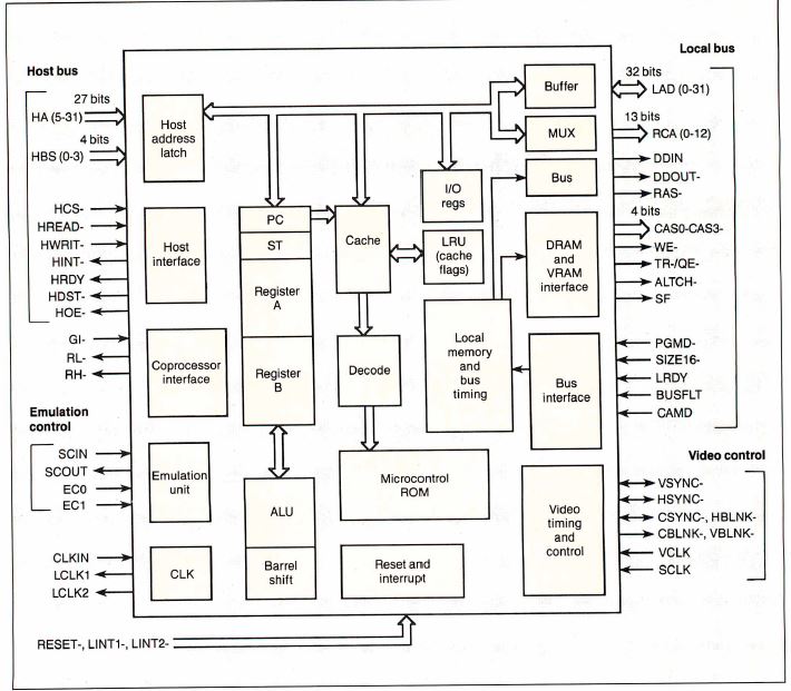
Figure 1: The TMS34020 block diagram
Note the coprocessor interface and the built-in host
attachment capabilities.
The '20 has all the architectural
features that define TI's TMS340 GSP family (see figure
1). These features include a host-bus interface, a
local-bus interface with semiautonomous memory controller,
a display-control interface and registers, instruction
cache, 31 32-bit registers, single-cycle general-purpose
instructions, and multiple-cycle graphics instructions.
(For details on the '10, see "The TMS34010 Graphics System
Processor" in the December 1986 BYTE.)
The '82 FPU is based on the same design
used by many bit-slice graphics workstation engines. It
directly connects to the '20's coprocessor interface and
has external expansion for both microcode and data.
The '20 has also been designed to take
full advantage of the features of the 44C251 1-megabit
VRAM. These improvements allow faster fills, masked
operations, and text without resorting to the expense of
the wide data buses used in many workstations.
Theory of
Evolution
The concept of a graphics engine
designed around a fully programmable microprocessor is
what made the '10 different from other graphics chips and
has led to the TMS340 family's success. The device differs
from a normal microprocessor in the special hardware and
microcode included to support bitmapped graphics
operations. It also integrates graphics system-control
features for the CRT, dynamic RAM (DRAM), and VRAM onto
one device. The underlying goal in this design was to let
the flexibility of bit-mapped graphics be matched by the
flexibility of a graphics processor.
The definition of the '20 began during
final development of the '10. Features that were too
expensive or that would cause major schedule delays on the
'10 were slated for implementation on the '20. The first
issue was to obtain an overall speed improvement over the
'10. This began with the obvious expansion of the '10's
32-bit internal and 16-bit external busing to a full32
bits for both on the '20.
With the addition of 32-bit pixel and
32-bit external bus support, several graphics features
have been enhanced on the '20. Pixel-formatted registers
are expanded from 16 to 32 bits in significance; these
include the color-expand registers and the plane-masking
register. Other enhancements include improving the
processor cycle time and utilizing the fast page mode of
DRAM. Also, the instruction cache was doubled to 512 bytes
on the '20 to reduce cache misses and let larger
algorithms fit into the cache.
New capabilities were also added.
Three-operand block transfers were needed by both
laser-printer manufacturers dealing with large textured
objects and system developers building extensive window
environments. Many system designers using the '10 had
requested better support for direct host access to the
TMS340's memory, and some of the more sophisticated
applications required the graphics processor to do
operations in the host 's memory space.
As a result, the host interface was
totally revamped for the '20. Better CRT timing control
was added to the display controller to enable
broadcast-quality RS170 National Television System
Committee (NTSC) timing. New XY addressing support
and improved VRAM control were also added to pack together
frame-buffer scan lines for better memory utilization. The
'20's VRAM support takes advantage of the 1-megabit VRAM's
split shift register as well as the older (and less
efficient) 256K-bit VRAM's midline reloading.
The '20 has enhanced the XY addressing support of
the '10 to include direct support for pitches
other than binary for the XY address space. (Pitch
is the distance between pixels on corresponding lines.)
Both pitches that are the sum of two powers of 2 (A
+ B where both A and B are powers
of 2) and completely arbitrary pitches are supported. This
makes the coding of output routines into linear memory and
instruction support for packed screen organizations much
easier. In addition, both X and Y values
on the '20 are treated as signed 16-bit numbers.
The definition of the '20 has gone far
beyond its own chip boundaries to include the development
of an extremely fast graphics floating-point coprocessor,
the '82. This processor is 30 to 100 times faster than the
typical microcomputer's FPU.
The Class of '82 [Text Box]
The 34082 is a high-performance
graphics floating-point coprocessor developed exclusively
for the 34020. Integrating a rnicrosequencer, register
file, floating-point ALU, and multiplier onto one chip
(see figure A), and supporting high-level graphics
instructions, the '82 can execute floating point
operations at up to 40 MFLOPS.
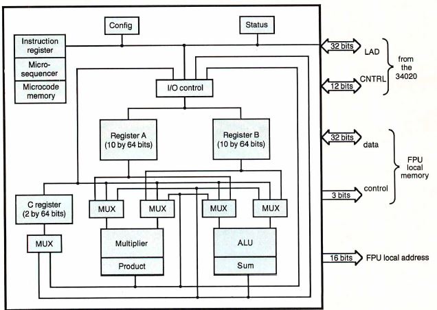
Figure A: TMS34082 floating-point coprocessor block diagram
Notice the 22 64-bit registers internal to the chip.
The register file on the '82 consists
of 22 64-bit registers. The file has 10 A-file registers
and 10 B-file registers for data storage and two C-file
registers for feedback. This large register file lets
complex algorithms store intermediate results internal to
the device, thereby reducing the memory cycles necessary
to reload these operands for future calculations. The
device also incorporates a local bus for storing up to 64K
32-bit words for data and microcode expansion. This
expansion memory lets you develop your own functions or
store data local to the '82.
Using the '20's coprocessor interface,
the '82 directly interfaces to the '20 with no "glue"
logic, letting the '82 be either initially designed into
the system or socketed for later addition. This interface
allows connecting up to four '82s to the '20. The '20
provides a general coprocessor interface to let the
external implementation of advanced functions improve
performance. The '82 is one example of a coprocessor
taking advantage of this interface for performance
increases. The interface consists of five basic cycles for
data communication and control:
- Move data from '20 register to coprocessor.
- Move data from coprocessor to '20 register.
- Move data from memory to coprocessor (indirect '20 register move).
- Move data from coprocessor to memory (indirect '20 register move).
- Execute coprocessor command.
Not only does it support fully
compatible IEEE Standard 754-1985 additions,
multiplications, divisions, square roots, and comparisons,
the '82 has instructions for complex graphics math.
Table A gives a complete list of instructions. And the
expansion capability of the '82 allows for the creation of
an indefinite number of user-defined functions.
The '20 project team also worked
closely with TI's memory-design engineers to allow the '20
to distribute some processing within the new 1-megabit
VRAM, the 44C251. (See the text box "Making Videos" on
page 272.) Coordination between the development programs
and the resulting cooperation between these three chips
enables simpler system design and higher performance.
Making Videos [Text Box]
The video RAM (VRAM) is a dynamic RAM
(DRAM) modified to let it transfer a large number of bits
from the memory array to a separate internal serial-shift
register. Prior to VRAMs, the majority of the available
bandwidth in conventional frame buffers (designed around
DRAMs) was used for display refreshing. This left
virtually no time for a processor to update the display.
After making the transfer, the contents
of the shift register are independently shifted out to the
display. As a result, the random port of the VRAM allows
unimpeded access to the graphics processor. With the
increasing resolutions of graphics displays and denser
memory devices, the VRAM is becoming indispensable to
frame-buffer design.
The original 64K-bit VRAM was organized
as a 64K-by-1-bit device and had a single 256-bit shift
register with four tap points (the starting column
position for the shift register). Memory
array-to-shift-register transfer cycles could be made only
during horizontal retrace when the serial clock to the
shift registers was stopped.
The next-generation VRAM was a 256K-bit
device that combined the functionality of four 64K-bit
VRAMs on a single chip. The device was organized into a
64K-by-4-bit device and contained four 256-bit
"serial-shift" registers. A static RAM and counter
emulated the shift-register function of its predecessor,
allowing the shift function to start from any tap point.
Transfers in the middle of a line were
enabled by changing the timing of the
shift-register-to-memory transfer. This "midline reload"
allowed designs to use fewer VRAMs for certain
frame-buffer sizes, but the timing was so critical that
few systems could take advantage of it. Furthermore,
various manufacturers experimented with features including
fast page mode, Boolean functions, and alternate
shift-register timing modes.
The latest VRAM generation is a
1-megabit device that has several architectural
enhancements to improve performance. The organization is
256K-by-4-bit with four 512-bit shift registers. Some
manufacturers plan an alternative 128K-by-8-bit VRAM. It's
important to note that when graphics architectures use
data buses wider than 128 bits, some memory devices will
be only partially used, because they need extra devices
just to reach the required data-bus width due to the
"deeper" organization of the by-4 memories. To compensate
for the increase in the depth of the memory, the 1-megabit
VRAM includes features to improve its performance without
requiring wider buses.
Most 1-megabit VRAMs support the
block-write mode (BWM), which gives a performance
improvement of four times or more on key graphics
operations, such as fills and color-text generation. Fast
page-mode accesses (common on 1-megabit DRAM) further
improve memory bandwidth. Some 1-megabit VRAMs will
support "persistent write per bit, "which lets color
masking be "locked in" on the VRAMs, reducing
read-modify-write (RMW) cycles. The 1-megabit VRAM will
also support "split-shift-register transfers," simplifying
the timing and control circuitry necessary for real-time
reloading of the serial-shift register. The split shift
registers provide memory savings in non-binary-powered
display resolutions.
BWM is the most significant new
architectural feature on the 1-megabit VRAM. On the
256K-by-4-bit VRAM, an internal 4-bit color register is
loaded from the 4-bit-wide data bus during a special write
cycle. At 4 bits per pixel, this latch contains the color
value to be written; at 8 bits per pixel, two VRAMs are
concatenated to form an 8-bit register.
When the VRAM's control signals select BWM, the two
least-significant bits of the address are ignored, and the
four "data pins" control the writing of the contents of the
color register into any or all of four consecutive locations
(a "block") in memory. A "1" on a data line initiates the
writing of the color register value, while a "0" prevents
that writing to the corresponding position in the block.
With four data lines controlling the four 4-bit memory cells
, the net effect is an effective increase of four times in
write bandwidth. The ability to support individual pixel
control in BWM allows this feature to be used for rendering
color text and area filling.
A Marriage of Convenience
Since the '20 and the 44C251 1-megabit
VRAM definitions were coordinated during development, the
'20 supports performance and system features added to the
44C251. The designers of the '20 had the advantage of
knowing and influencing the definition of the VRAM, so the
two architectures fit together.
The importance of that joint definition
can be seen most clearly with the blockwrite mode (BWM).
The 44C251 has four banks of 64K -by-4-bit memory, for a
total of 16 bits wide internally (see figure 2a).
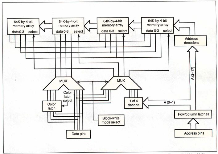
Figure 2a: TMS44C251 VRAM internals
Notice the four banks of64K-by-4-bit
memory,for a total internal width of 16 bits.
In normal mode, the two least significant bits of the
address select one of four banks-only one can be selected
at a time-and the four data lines provide the data. In
BWM, the four data lines used enable writing to any and
all combinations of the four banks within each 44C251, and
the special color-latch data is multiplexed to provide the
data when it's written. The '20 controls the 44C251 to
expand the 32-bit data path to 128 bits wide inside the
VRAM (see figure 2b).
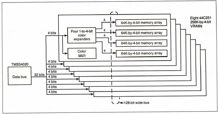
Figure 2b: 44C251 and its connection to the '20
Notice how the '20 expands the 32-bit data path to 128
bits wide inside the VRAM.
The BWM function is modeled after the
TMS340 family's "binary to color expand" function. Color
expansion works by turning data into control signals that
select whether or not to write a color. Since each data
line controls a multiple-bit color value, we use the term
"color expansion."
Both the ' 20 and the '10 have flexible
color expanders that turn 1-bit-per-pixel shape
information into 1, 2, 4, 8, or 16 bits per pixel. The '20
extends this function to 32 bits per pixel. This function,
widely used in bit-mapped color graphics, would be very
tedious without hardware help
Although the BWM has the potential to
give an additional performance increase of four times or
more for fills and color text , it requires special
addressing and control- and data-mapping hardware built
into the '20. The mapping hardware makes writing pixels
into the memory consistent with how they would be written
without BWM and can be thought of as the "key" that
unlocks the block-write feature.
When using the BWM, you can think of
each 44C251 VRAM as having four 1- to 4-bit fixed color
expanders in it; in other words, each memory can expand 4
bits of incoming data or control information into 16 bits.
By combining two VRAMs (to get an 8-bit-wide color latch
and expander), you can get four 1- to 8-bit expanders.
By using the '20's color-expander
hardware plus additional on-chip hardware to generate the
control signals necessary to interface to the VRAMs, the
'20's 32-bit data bus is effectively expanded to 128 bits
during BWM cycles. The '20 also supports the color-expand
functions for complex graphics math. Table A gives a
complete list of instructions. And the expansion
capability of the '82 allows for the creation of an
indefinite number of user-defined functions. function for
memories without BWM, which still gives an improvement
that is roughly 10 times that of microprocessors without
color-expand hardware.
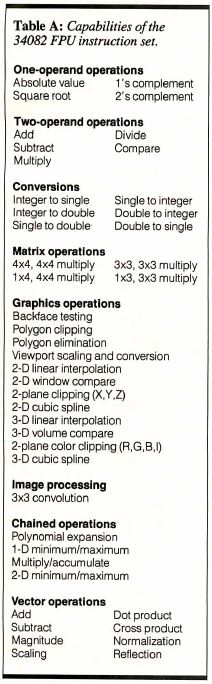
Table A: Capabilities of the 34082 FPU instruction set
Two special instructions were added to
the '20 to take advantage of the BWM. VFILL is
used for fast solid filling. The VBLT
instruction reads binary shape information and controls
the VRAM for text and pattern color expansion.
Another area of improvement is in the
plane-masking function. The 44C251's "persistent write per
bit" speeds up this function. The '20 doesn't have to do
read-modify -write (RMW) cycles to perform the masking
operation.
By combining the wider data bus, fast
page mode, faster processor cycle , and BWM support on the
'20, you get a performance advantage of up to 50 times
over the ' 10 when writing color text. Remarkably, the
'10's internal color expand hardware already gave it a
significant advantage over general-purpose processors at
this function.
The 44C251's split shift register
greatly simplifies the timing requirements for loading the
shift register while it's still allowed to shift. The
special control and timing are directly supported by the
'20, removing the time-critical real-time reload headache
from the system designer.
Strike Up the
Band
The ' 20 significantly increases the
system-bus bandwidth of the '10 due to improvements in
three basic areas: a wider data bus (32 bits on the '20
versus 16 bits on the '10), exploiting enhanced page mode
accesses on DRAMs and VRAMs, and a faster clock speed or
state rate. The wider data-bus and page-mode accesses let
the '20 fetch more instructions in less time on a cache
miss. And, at a clock speed of 40 MHz, the '20 typically
fetches 16 instructions in 900 nanoseconds, while a 50-MHz
'10 fetches only3. Together, these improvements provide
performance increases of three to seven times on the '20
when executing programs written for the '10.
The largest performance increases due
to local-bus bandwidth improvements, however, come in the
multiple-cycle data-manipulation instructions. The '20's FILLs,
PIXBLTs, and BLOCK MOVEs have improved
the most. For example, a fill operation on the '20 paints
the screen in one-seventh the time required by the '10;
you can get even more dramatic performance increases, up
to 50 times that of the '10 , if you use the block-write
capabilities of the 44C251 VRAM. For large data transfers,
the '20 incorporates an eight-word (32 bits per word)
first-in/first-out that scoops up the source data,
modifies it, and returns it to the destination within
local memory.
Another unique feature of the '20 is
the four CAS- outputs (see figure 1) that support
byte-write operations, thus avoiding RMW cycles. Many
graphics and string operations require intensive byte
manipulation provided by the '20's CAS- strobes.
Furthermore, these strobes let the '20's line-drawing
engine splatter the display with 5 million pixels in a
single second (RMW cycles would reduce performance to less
than 3 million pixels per second).
In addition, the '20 dynamically sizes
to 16- and 32-bit-wide memories via the SIZE16- input;
simultaneously, the '20 can dynamically change its column
and address multiplexing to support memories of different
array sizes in the same system without additional
hardware.
Hosting the
Affair
The '20 operates as either a host
processor or a graphics processor attached to a host bus.
The host interface on the '20 is completely transparent to
the host system. When the '20's memory is mapped directly
into the host system's memory map, the '20 functions as a
DRAM controller.
On a host access to the '20's local
memory, the host's address is latched into the '20. The
address is then reformatted and presented on the LAD and
RCA buses to the '20's local memory (see figure 1). Data
is routed via external data buffers that are directly
controlled by the '20.
The 38-pin interface supports burst
rates of up to 20 megabytes per second in either
block-transfer or random-access mode. The '20 provides
option bits in the internal host control register to let
the interface pipelining be configured for block (read or
write) or RMW operations for maximum performance.
The '20 supports multiprocessing
environments and can access host memory directly to
improve system performance when accessing host resources.
Built-in bus-fault and retry mechanisms handle address
violations and bus-contention conditions. The '20 supports
data: operations in big endian (data indexed from
the most-significant data bit) and little endian
(data indexed from the least-significant data bit) modes,
thus removing swizzling (data remapping)
operations.
Hold That Line
The '20's Hold/Holda protocol not only
lets another processor suspend the master GSP from
operating on its local bus, but also lets other GSPs be
directly wired onto the same local bus . Three signal
lines-grant in (GI-), low-priority request (RL-), and
high-priority request (RH-)-provide the handshake
mechanism on this interface (see figure 1). These three
lines are necessary to handle special problems associated
with both graphics systems and DRAM- and VRAM-based
systems.
In a typical Hold application, the '20
must reassert bus control if a shift-register-transfer
(display-refresh) or memory refresh cycle is pending.
Internal counters schedule latency of these events to
provide maximum performance. Internal refresh queuing of
up to 12 DRAM refresh cycles limits bus re-arbitration.
Two or more '20s can be directly wired
together to increase system performance. Multiple GSPs
synchronized to the same local clock can efficiently
handshake over the three-wire interface, allowing control
of the bus to be passed between processors on every local
memory cycle. With the increased size of the instruction
cache and the improved efficiency of instruction
acquisition, a significant performance increase can be
obtained by using this interface.
Learning the
Rules
The '20 has built on the '10's full
suite of general-purpose instructions and combined them
with a rich set of application specific graphics
instructions (see table 1). Note that the processors have
a sufficient set of the necessary assembly language
instructions to support a robust C language with direct
field support.
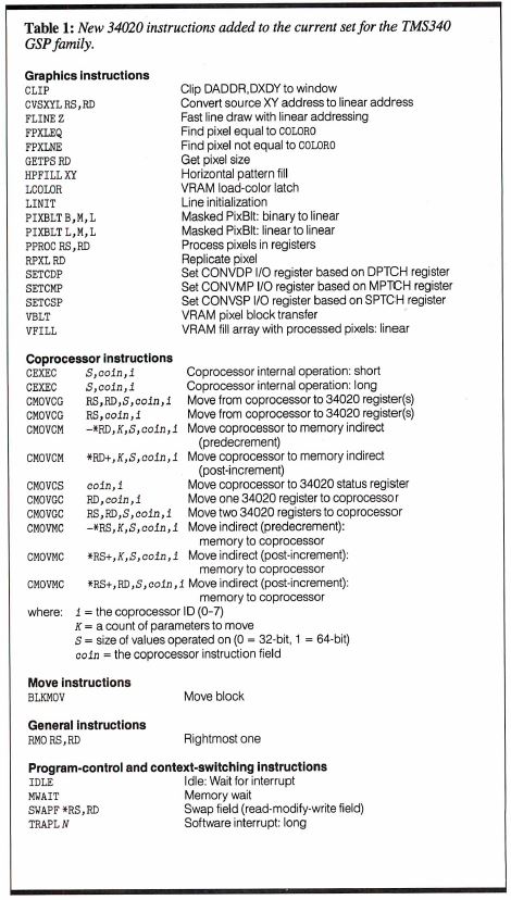
Table 1: New 34020 instructions added to current set for TMS340 GSP family
Both the '10 and the '20 have direct
support for operations on fields in memory. Since they are
bit-addressable processors, fields in memory can start on
any bit boundary; the instruction set further supports
varying field widths (from 1 to 32 bits). This can be
especially important in manipulating C "fields" and in the
memory storage required for packed arrays in C. The TMS340
family's hardware support for fields augments these
operations. (Pixels are a special case of regularly sized,
packed fields in frame-buffer memory.)
Two-operand pixel-block-transfer
instructions (PIXBLTs) perform 16 binary and 6
arithmetic raster operations on a pair of two-dimensional
pixel arrays. The two-operand PIXBLTs are useful
for manipulating and moving bounded objects and operating
with solid color.
You can simulate more elaborate
operations using multiple PIXBLTs, arithmetic
raster operations, and the 10's binary-expand operations.
Using the binary expand, fonts stored as bit patterns form
color text (with transparency), and two-color patterned
operations can be performed on the bit map. The
flexibility of the PIXBLT instructions lets you
build operations such as the 8514/A's compare operations,
as well as foreground and background raster operations. In
addition, you can build support for non-rectangular
objects on top of two operand PIXBLTs.
The ' 20 extends the '10's PIXBLT
instructions by adding a third operand, a binary-mask
operand. While the '10 supplies hardware support for
rectangular window regions and pixel blocks, many
applications have begun to require control and rendering
of non-rectangular window regions. The third mask array
supports this feature on the '20. The mask is used to
describe the window region on a pixel-by-pixel basis. This
provides complete flexibility in describing a region: It
can be filled, concave, convex, outlined, have holes, and
so on.
The three-operand PIXBLT employs the
binary-mask array to act on the first operand, the
source-pixel array. This mask array selects individual
pixels in the source array to be combined with the
destination array (an independent operand). For text, the
source array can be an arbitrary pattern (dithered or
halftoned) describing the "color" or "shading" of the text
(see figure 3). The mask array contains the description of
the shape of the character, or glyph. The destination
array is the displayable "canvas" onto which the character
is painted.
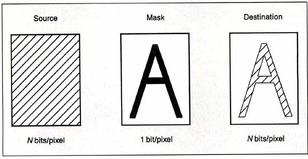
Figure 3: The three-operand PIXBLT
In this way, the bits having a value of
1 in the mask select pixels (1, 2, 4, 8, 16, or 32 bits
deep) in the source-array pattern to transfer to the
destination location. There is the additional option of
performing one of 22 raster operations on the selected
source or destination pixels, as well as several
transparency and plane-masking options.
See- Through Pixels
Raster operations on the TMS340 family
include all the Boolean combinations of 2 bits and their
complements, plus an arithmetic set. This latter set
supports addition and subtraction of pixels as well as a
unique pair of comparison operations. The first computes
the maximum of the source and destination pixels. The
second computes the minimum pixel value. These operations
are useful for layering "planes" of data via the
intelligent ordering of pixel indexes or colors. They have
been used to "drag" sprite-like objects around the screen
without corrupting background or foreground images. Pixels
are combined through binary or arithmetic raster
operations to form a resultant pixel.
Raster operations for the '20 contain
several new transparency modes. Transparency is the notion
that there are cases in which it is useful to inhibit the
writing of new pixel data to the destination based on
information within the actual operands of the raster
operation. Thus, transparency circumvents the normal
determination of what value is to be written to the
destination pixel.
The four '20 transparency modes are
transparency inhibited, transparency on resultant pixel =
0, transparency on source pixel = 0, and transparency on
destination = COLORO . The first two are '1
0-compatible modes.
When transparency is inhibited, raster
operations proceed as normal. For transparency on the
resultant pixel equal to 0, the '20 checks the pixel value
that results from the raster combination for zero-valued
pixels. The zero value is then replaced with the original
destination-pixel value so that the destination-pixel
location is not changed.
For transparency on the source pixel
equal to 0, the source-pixel value is checked before the
raster operation for zero-valued pixels. Each zero value
is identified so that the destination pixel retains its
original value. This is useful for maintaining transparent
pixels in the source-pixel array while using other '20
raster operations.
For transparency on the destination
equal to COLORO, the destination-pixel value is
checked before the raster operation for pixels that equal
the "background" color (stored in the 32-bit COLORO
register). Each background value pixel in the destination
is not modified by the raster operation. This is useful
for maintaining background pixels in the destination bit
map, regardless of the value of the source pixel and which
of the 22 raster operations are enabled.
Working on the Line
Several design areas on the '10 in the
area of line support were targeted for enhancement on the
'20. Among these were fast line draw, line initialization,
and support for patterned lines and arrays.
To enhance line-draw performance, the
'20 has added a fast line-draw instruction to the '10's
Bresenham-algorithm line draw (see "Better Bit-Mapped
Lines" in the March BYTE). This FLINE
instruction performs the same arbitrary angle algorithm
found on the '10, but it assumes pre-clipped endpoints as
input. This allows the CPU to bypass the window-checking
microcode and execute the heart of the line-draw algorithm
at memory-bandwidth speeds (raster operations, plane
masking, and transparency are all active).
To reduce overhead during line
initialization, the LINIT instruction performs
the necessary setup for the LINE instruction. LINIT
speeds up and simplifies the operation overhead associated
with line initialization. More important, LINIT
allows larger algorithms utilizing the LINE
instruction to fit into cache, thereby increasing
drawing performance.
For enhanced patterned-drawing support,
the '20 adds a horizontal-fill instruction, HFILL, which
supports patterns described in a 32-bit internal register.
The repeating pattern is taken from the register and
rotated as pixels are drawn if the register contains a
nonzero pattern. The PATTRN register contains
the current drawing position in bit 0 at the end of the
instruction.
But Can I Use It?
The '20 offers a full line of
development tool support built on the '10 support
environment. A full Kernighan and Ritchie optimizing C
compiler utilizing many of the extended features of the
TMS340 architecture is available. Supporting the C
language environment is a full set of assembly language
tools for building relocatable, ROMable, or all-RAM
executable files. A TMS340 family common
object-file-format (COFF) loader, C 110 package, and high
-level-language debug support are planned for the '201
The '20 is object code-compatible with
the '10. This means that math libraries, graphics
libraries , graphics interfaces, and graphics-standards
software are already available for the '20. These will be
enhanced over time to use the extensions of the '20.
A Family Reunion
With the entrance of the '20 and '82,
the TMS340 architecture addresses a very wide range of
graphics applications. The '10's smaller package size and
high level of system integration is ideally suited to
high-volume cost-sensitive applications. The more powerful
'20 provides an upwardly compatible migration path for '10
designs and meets the needs of higher performance systems.
By adding a TMS34082 Graphics
Floating-Point Unit and TMS44C251 VRAM to a 34020-based
system, a small board can have all the graphics and math
capabilities of a high-end workstation.
Ron Peterson, Carrell R. Killebrew
Jr., Tom Albers, and Karl Guttag are all members of Texas
Instruments' design team for the 34020. They can be
reached on BIX as "editors."
|