|
rf855657.exe 8556/8557 Reference Disk v2.10 (zipped image)
Reference disk supports SLC2/SLC3 upgrades.
rf855657_v123.zip Reference Disk v1.23 (31 Jan 1992, 10G6297)
![[P]](/other/img/photo.gif)
Old version! Includes diagnostics. Cleaned up image. (thx to John Horvath)
rf8557um_v123.zip Ultimedia M57 SLC Reference Disk v1.23 (12 Dec 1991, 10G4222)
Possibly not the latest version. Includes diagnostics. (thx to John Horvath)
rf8557um_v123_alt.zip Ultimedia M57 SLC Reference Disk v1.23
Same contents as above except for 4 bytes in the boot sector. (thx to John Horvath)
rd855657.exe 8556/8557 Advanced Diagnostics v2.04 (zipped image)
191-078 PS/2 MODEL 57 SX (8557-045 AND 049)
192-059 PS/2 ULTIMEDIA MODEL M57 SLC (8557-259)
486SLC CPU Upgrade
486SLC2 CPU Upgrade
486SLC3 CPU Upgrade
Cached CPU Upgrade
8556 / 8557 Planar
Early SX Planar
Later SX & Early SLC Planar
Late SX & SLC Planar
System Firmware
ROM Images
Riser Cards
Specifications
VRAM Functionality?
8556 / 8557 Planar
Early SX Planar
386SX 20 MHz: FRU P/N 84F7994, P/N 04G3815
(photo from UMMR)
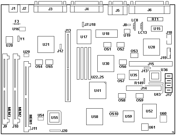
F3 Keyboard/mouse fuse
J1 Mouse port
J2 Keyboard port
J3 Parallel port
J4 DB25 serial port
J5 HDD15 video connector
J6 C60 External SCSI port
J8 Pads for 2-pin jumper
J7/J18 Password-override jumper
J9-11 72-pin SIMM socket
J12 Pads for 3-pin header
J13 MCA riser slot
J13* Pads for 3+1-pin SCSI diag. header?
J14 44-pin floppy connector
J15 50-pin SCSI connector
J17 Power-supply connector P1
J18 Control-assembly connector
J19 Power-supply connector P2
J20 Pads for 6-pin header (+key)
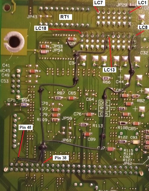
LC8,13 3-pin PCB module (bodge)
OS1 28.3220 MHz osc (SVGA)
OS2 41.5390 MHz osc (SVGA)
OS3 32.0000 MHz osc
OS4 22.1184 MHz osc (UART)
OS5 14.3181 MHz osc (adapters)
OS6 25.1750 MHz osc (SVGA)
OS7 Pads for 44.9 MHz osc (SVGA)
|
OS8 40.0000 MHz osc (CPU)
OS9 24.0000 MHz osc (FDC)
OS10 Pads for 40 MHz osc (CPU?)
R149 PTC fuse
RT1 SCSI Termpack "T-Res"
U15 CXK58267AM-12L 32Kx8 SRAM (NVRAM)
U16 Pads for DIP-8?
U17 85F0120 SVGA #2
U18 Inmos IMSG171P-50 RAMDAC
U19 Dallas DS1210S NVRAM controller
U20 Dallas DS1285Q RTC/CMOS
U21 91F7490 I/O controller?
U22-25 64Kx16 DRAM (video)
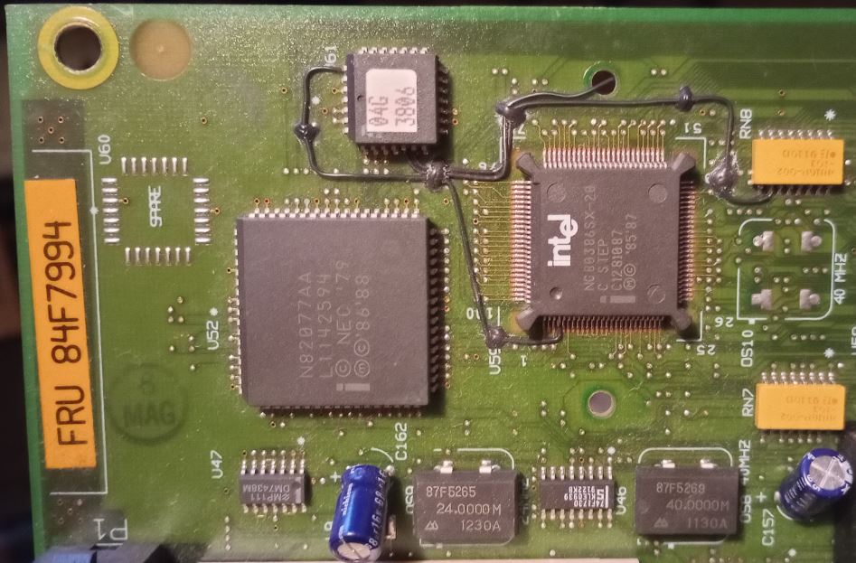
U28 64F4760 SCSI ctrl. "Jalpa" (local bus)
U29,54,60 "Spare"
U30 84F7985 SVGA
U35 Siemens 8032B-16 MCU (SCSI)
U36 SCSI microcode ROM 92F1211
U41 121-pin upgrade/387SX socket
U43 Pads for 9-pin part
U52 82077AA Floppy controller
U55 92F1600 POST/BIOS ROM
U58 92F1495 System controller?
U59 i80386SX-20 or IBM 386SLC-20 CPU
U61 04G3806 or 10G7706 PAL
Y1 32.768 KHz xtal (RTC)
|
J7 has a little sticker over it that
says "J18".
J13* Pads for 3+1-pin SCSI diag. header?
Possibly the same pinout as J22 on the 9556/7 planar.
If correct, this port can be used to access the
Serial Console.
LC8,13 3-pin PCB module; Soldered in
place of ferrite beads and accompanied by a set of
bodge wires (and most
likely cut traces) on the solder side (thx Louis). The modules intercept the
-REQ and -ACK signals going from the SCSI controller to the internal and
external SCSI connectors. Each PCB module contains a mix of active and passive
components. It's unknown how exactly are the two SCSI signals manipulated. The
LC8 PCB is P/N 92F1551, the LC13 PCB is P/N 92F1552. Later boards have
dedicated positions for these modules (with one of them seemingly implemented
directly on the board).
U22-25
Toshiba TC511665Z-80H (or BZ-80)
64Kx16 DRAM 40-pin ZIP video memory. See HERE.
U41 The 121-pin PGA socket can be used
to install either a CPU upgrade module or 68-pin PLCC socket for 387SX or
compatible math coprocessor.
These early boards have a rework in the processor area involving CPU pin 4
(and possibly one other), PAL U61 and
resistor network RN8. See detail photos
HERE and
HERE (thx Louis). This
should not be confused with the CPU rework wires present on
Early SLC Planars.
Later SX & Early SLC Planar
386SX 20 MHz: FRU P/N 84F7994, P/N 10G4876
386SX 20 MHz: FRU P/N 79F7211, P/N 95F3564 (FRU sticker over silkscreen)
386SLC 20 MHz: FRU P/N 85F0298, P/N 10G5020
(SuperVinx photos)
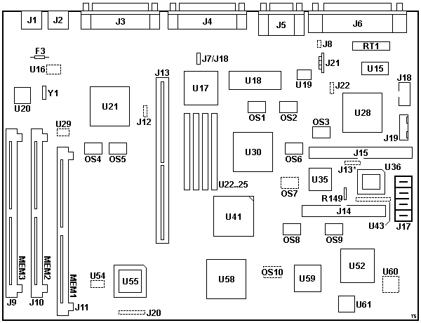
Same as the Early SX Planar above with some
layout differences. Notably:
LC8,13 Ferrite bead (not marked on the outline)
J21 3-pin PCB module
J22 Pads for 3-pin PCB module?
The SLC variant has a set of four bodge wires in the CPU area involving pins
44, 46, 47 and 30 (?). This should not be confused with the CPU rework wires
present on Early SX Planars.
Late SX & SLC Planar
386SX 20 MHz: FRU P/N 84F7994, P/N 92F2513
(SuperVinx photos)
386SLC 20 MHz: FRU P/N 85F0298, P/N 10G7645
(SuperVinx photos)
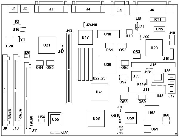
Same as the Later SX & Early SLC Planar
above except for:
JP94-97 0-ohm resistors (SLC) or pads only
(SX). This replaces the bodge wires from the Early SLC
Planars.
System Firmware (POST & BIOS)
Firmware stored in EPROM.
ROM Images
92F1600 - Unknown date/revision (sticker date 16/09/91)
96F7567 - Unknown date/revision (seen in M57SLC) (sticker date 24/02/92)
96F7568 - Unknown date/revision (same as above?) (seen on Early SLC Planar) (sticker © 1991)
10G5029 - 07 Dec 1991, rev. 9 (sticker date 13/10/92 or 22/05/92)
All are 1x Am27C2048-150JC (U55).
Riser Cards
8557SX Bus Adapter
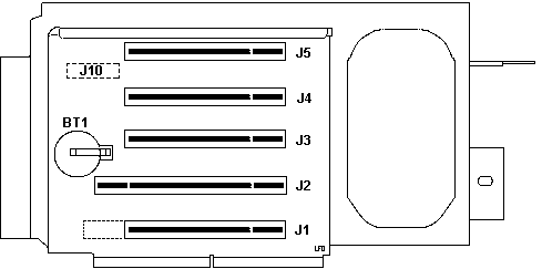
Dotted area on J1 Solder pads for a BVE segment
J10 Solder pads for a 16 pin header
J2 AVE slot
If you have a fantasy about swapping a Lacuna riser and planar into your
57SX, forget it. The Lacuna riser has two mounting slots where the screws are
both horizontal, while the 57 has a vertical screw and a horizontal screw. The
lacuna mounting holes at the front don't match.
Specifications
The 57SX supports up to 16 MB of 70 ns memory (all DMA addressable) on the
planar in three SIMM sockets. The memory controller automatically supports
enhanced performance via memory interleaving with all 2 MB or all 4 MB SIMMs.
One, two or three 2 MB SIMMs provide memory interleaving. Two or three 4 MB
SIMMs also provide memory interleaving. The 8 MB SIMMs do not provide
interleaving.
Video is provided via the enhanced 16-bit industry-standard VGA.
Supports 720 KB, 1.44 MB and 2.88 MB diskettes.
VRAM Functionality?
> This one has actual sockets installed though, not empty pads...?
Peter says:
Yeah, most have them, and they are somewhat connected to the
video-chip glue logic on the planar. But basically they are non-functional. If
you look on the board you will find the same old boring Inmos RAMDAC as on
Models 50/60 55/65 70/80, with limited bandwidth. Just enough for standard-VGA
or 320x200 / 256 colors CGA mode. And - as said: the machine lacks the video
modes in its BIOS AFAIK.
Some of the later Greenock variants of the 8556/8557 planar even lack these
sockets and have only soldering spots. That was what my comment referred
on.
You might however try to install some chips there for 512K and see if you
can enable the mode 2Eh - that's 640 x 480 / 256 colors from a 256K palette at
60Hz vertical / 31.5 KHz horizontal. The system should choke out at Mode 12h
(640 x 480 / 16 out of 256K, 60Hz / 31.5 KHz) and 13h respectively (320 x 200 /
256 out of 256K, 70Hz / 31.5KHz).
| 