|
M6-5x0_ref105.zip M6 520/540/560 Reference Disk v1.05 (C&T Setup Program v3.61)
![[P]](/other/img/photo.gif "Splash Screen")
Bootable image, restored using Reply TurboProcessor 60/80 system files.
M6-540_bios.zip M6 520/540/560 Reference Disk v1.05 files (C&T Setup Program v3.61)
Non-bootable, zipped files only, Win95 system files.
mach32 Drivers and Utilities
Pocket Service Guide - M6-520/540/560 (selected pages only)
System Software Configuration (Setup Utility)
Specifications
M6-5x0 Planar
SW1 DIP Switches
System Firmware
ROM Images
BIOS Revision Levels
Front Panel Connector
Expansion Bus Riser
Power Supply
Planar Power Connector
Specifications
CPU: Depending on the model:
M6-520: i486SX @ 25 MHz soldered in, upg. socket available
M6-540: i486DX @ 33 MHz socketed
M6-560: i486DX2 @ 33/66 MHz socketed
Pentium OverDrive (P24T) available as an option
Memory: 4x 72-pin SIMM slots, 8 - 64 MB, 70 ns
Bus: 3x 32-bit MCA slot on a riser (one with AVE)
Video: ATi mach32 VGA (on-board), 1 MB video RAM
HDD: on-board SCSI, 120 - 1050 MB drives
FDD: 3.5" 2.88 MB (34-pin, Sony MP-F40W-17, -17/1)
I/O: PS/2 keyboard & mouse, 2x 9-pin serial, 1x parallel
M6-5x0 Planar BA2096 (M6-520 w/ QFP 486), BA2097 (M6-540/-560 w/o QFP 486)
"COPYRIGHT (C) REPLY, 1993", "P.C.B. cod. 654213E 29/11/93"
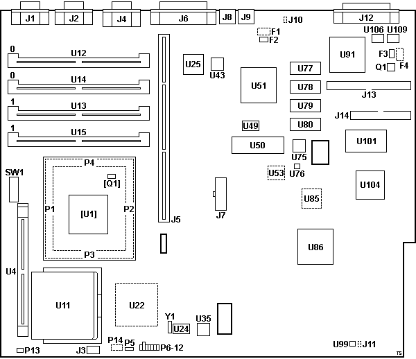
F1 Pads for alt. KB/mouse? fuse
F2 3 A/125 V KB/mouse? fuse
F3 1.5 A/125 V SCSI fuse
F4 Pads for alt. SCSI fuse
J1 DE9 serial port 1
J2 DE9 serial port 2
J3 6-pin front panel connector
J4 HDD15 video connector
J5 Bus riser slot
J6 Parallel port
J7 12-pin power connector
J8 Keyboard port
J9 Mouse port
J10 Pads for 2-pin header (shorted)
J11 Pads for 2-pin header (shorted)
J12 External SCSI Connector
J13 50-pin SCSI Connector
J14 34-pin floppy header (industry std.)
P1-4 "Mad River Module" headers
P5 SCSI terminator enable
P6 2-pin jumper
P7 Power on password clear
P8 Floppy write enable
P9 Serial/parallel port enable
P10 2-pin jumper
P11 Serial boot enable
P12 Floppy boot enable
P13 2-pin fan connector (12 V)
|
P14 pads for 2x4-pin header (JTAG?)
Q1 SCSI term. transistor?
SW1 DIP switches
U4 L2 Cache Socket
U11 Socket 3 ZIF
U12,14 72-pin SIMM sockets Bank 0
U13,15 72-pin SIMM sockets Bank 1
U22 Pads or QFP 486SX (M6-520)
U24 IC Designs ICD2027SC-1 clock gen.
U25 Bt481KPJ85 or Bt481AKPJ110 RAMDAC
U35 40.000 MHz osc
U43 M60022-1002FP "EYE"
U49 ATI18811 ICS2494AM clock gen. (VGA)
U50 28F010 128Kx8 Flash EPROM (DIP-32)
U51 ATi 2106880006 ("68800") mach32
U53 Pads for alt. Flash EPROM (PLCC-32)
U75 22.1184 MHz osc (UART)
U76 LT1109-12 DC/DC conv. (Flash Vpp)
U77-80 256Kx8 VRAM (1 MB total)
U85 Pads for backup EPROM? (PLCC-44)
U86 NCR 53C700-66 SCSI controller
U91 10G4672 I/O controller
U99 LM386 Audio op-amp (PC Speaker)
U101 Dallas DS1387 RTC+NVRAM
U104 82077SL-1 Floppy controller
U106,109 Dallas DS2107A SCSI Terminator
Y1 14.318 MHz xtal (clock gen., adapters?)
|
U77-80
Hitachi HM538253J-8,
Micron MT42C8255DJ-8, or
compatible 256Kx8 VRAM (1 MB total).
U86 NCR 53C700-66 SCSI controller
NCR 53C700 SCSI I/O Processor Data Manual, Feb 1990
NCR 53C700 SCSI I/O Processor Data Manual, Nov 1992
NCR 53C700 SCSI I/O Processor Programmers Guide, Mar 1990
The rest of the board is covered with 74xx glue, a few PLDs, and a bunch of
passives.
Mad River Module "ASSY 05003300 REV B", "(C) 1993 REPLY CORP"
[U1] 50G6871 SynchroStream Controller
[Q1] LT1117 voltage reg., 800 mA max. (for SynchroStream)
The module has 419 pins total (420 - 1 key). 2 mm pitch.
Why is the SynchroStream controller on a daughter board? It may sound
counter-intuitive, but my SWAG is it was done as a cost-saving measure. To
"fan-out" all the connections, the CBGA-625 package asks for a PCB with a
relatively high layer count and/or very thin traces. The other ICs are nowhere
near as demanding, so it would be a waste to use that many layers/level of
precision for the entire system board.
The name "Mad River" is mentioned in the
Pocket Service Guide - M6-520/540/560
(page 4 physical).
SW1 DIP Switches
| SW | Function | Setting | Description |
|---|
| 1/2 | Selects the type of drive with floppy disk interface (Drive A) | ON | ON | 3.5", 1.44 MB floppy disk drive
Not available |
| OFF | ON | 3.5" 2.88 MB floppy disk * |
| ON | OFF | 5.25" 1.2 MB floppy disk drive
Not available |
| OFF | OFF | 80/120 MB streamer
Not available |
| 3/4 | Selects the type of drive with floppy disk interface (Drive B) | ON | ON | 3.5", 1.44 MB floppy disk drive
Not available |
| OFF | ON | 3.5" 2.88 MB floppy disk * |
| ON | OFF | 5.25" 1.2 MB floppy disk drive
Not available |
| OFF | OFF | 80/120 MB streamer |
| 5 | — | OFF | Not used |
| 6 | — | OFF | Not used |
| 7 | System clock | ON | 25 MHz (M6-520) |
| OFF | 33 MHz (M6-540 / M6-560) |
| 8 | EPROM write enable | ON | EPROM write is enabled. The BIOS can be updated using the appropriate USer Diskette utility. |
| OFF | EPROM write disabled |
* Default setting
System Firmware (POST & BIOS)
Firmware stored in Flash EPROM (28F010, DIP-32 or PLCC-32).
ROM Images
R1_47_36.zip - Reply Corporation BIOS Version R1.47.36
Dumped from a functional system. Non-zero seg. F000 checksum.
Contains ATI68800 MCA3212.02 video BIOS.
Contains NCR SDMS 53C700-66 REP766M-3.00.24 SCSI firmware.
BIOS Revision Levels
X0.36.27
Original release?
X0.37.30
Corrects some of the faults encountered during the testing phase in the different
operating environments.
R1.47.32
Corrects some of the faults encountered during the testing phase in the different
operating environments.
R1.47.36 (14 Jun 1994)
This new BIOS version corrects the following faults:
- Problems encountered in the MOREMEM.COM program code
- Problems with OS/2 when a second floppy diskette drive is installed
- Problems in managing more than three serial ports
Front Panel Connector
Planar Connector Pinout
| Pin |
Description |
| 1 |
Speaker |
| 2 |
Ground (speaker, power LED?) |
| 3 |
HDD LED+ |
| 4 |
HDD LED- |
| 5 |
N/C? |
| 6 |
Power LED+? |
Connector Type
Molex Picoflex 90327 Series, 6 pins
Expansion Bus Riser IN2004
3x 32-bit MCA slot, one with AVE.
Power Supply
Magnetek
Type PS11 STD
Code: 3444-14-001
Made in Italy
Input:
100-125 V AC 4.5 A 50/60 Hz
220-240 V AC 2.4 A 50/60 Hz
AC Output:
100-125 V 2 A 50/60 Hz
220-240 V 1 A 50/60 Hz
DC Output:
+5 V 18 A
+12 V 3.0 A
-12 V 0.3 A
Planar Power Connector
Planar Connector Pinout
|
|
| |
Pin(s) |
Description |
Notes |
| |
1,2,3 |
+5 V DC |
|
| |
5,6,7,8 |
Ground |
|
| |
10 |
+12 V DC |
|
| |
11 |
-12 V DC |
|
| |
12 |
Power Good |
+5 V if all voltages are stabilized |
|
Connector Type
Molex Mini-Fit Jr., 5566 Series, 12 pins
Planar Header:
39281123, 39288120, or equivalent - Mini-Fit Jr. Vertical Header, 4.20mm Pitch, Dual Row, 12 Circuits, without Snap-in Plastic Peg PCB Lock, Tin, Natural
PSU Receptacle:
39012120, 39012125, or equivalent - Mini-Fit Jr. Receptacle Housing, Dual Row, 12 Circuits, Natural
|