|
Table of Contents
[-0-] Version History, Disclaimer & Legal Info
[-1-] Precautions and Warnings before you start
[-2-] Introduction to the Type 4 "Y" Pentium 90 Platform
[-3-] The importance of cooling certain components
[-4-] Modification A) Using a Pentium Overdrive 180 / 200
[-5-] Modification B) Hardwiring the BF0 / BF1 Pins for different Bus / Core ratios
[-6-] Modification C) Changing the Base Clock from 60 to 66 MHz
[-7-] Modification D) Using a Pentium MMX 233 MHz with an Interposer
[-8-] Problems, Workarounds and other stuff
Content by Peter H. Wendt (original HERE). Edited by Major Tom.
Modification D) Using a Pentium MMX 233 MHz with an Interposer
Let's start with some CPU basics.
Do I have a MMX or Classic (non-MMX) Pentium?
First check the writing on the top side of the CPU:
Classic (non-MMX) Pentium chips are labeled Intel pentium ixxx.
MMX Pentium chips are labeled Intel pentium w/ MMXtmtech.
Where xxx is the speed rating (i.e. 166 or 200).
Sometimes it's difficult or impossible to read the writing on the top (glued
heatsinks etc.), in which case you can identify it by checking the underside:
Classic (non-MMX) Pentium chips are labeled intel pentium FV80502xxx
MMX Pentium chips are labeled intel pentium w/ MMX tech FV80503xxx
Where xxx is the speed rating. Part number starting with 80502
signifies a non-MMX chip (P54C/CS/CQS), and 80503 signifies a MMX part
(P55C).
Most MMX chips came in the newer plastic package (PPGA, black base with
silver heat spreader), but some of them used the ceramic package (CPGA) typical
for older processors (classic Pentium, 486, 386DX...). But the "MMX tech"
marking should always be clearly visible - on the top as well as on the
underside.
Please note that some later non-MMX chips also used the black plastic package
- namely Pentium 166 and 200.
Warning: Never try to install a Pentium MMX
CPU on the P90 platform directly!
The MMX chips use a split-voltage design where the processor core runs at a
lower voltage (i.e. 2.8 V) than the I/O portion of the chip (that runs at 3.3 V).
Using the chip on a straight 3.3 V platform is not a good idea. The chip will
produce excessive heat and the overvoltage may degrade or destroy the chip!
You need to use a special adapter - so called
interposer
- with a secondary power regulator, which reduces the core voltage to an
appropriate level. This regulator isn't powered through the CPU socket
on the motherboard/processor card, but directly from the main power supply. This
is necessary to satisfy current requirements of the higher-clocked chips. Many
older Socket 5 boards were not designed for this kind of power draw.
One of these adapters is the Madex 486007 kit. It consists of two parts:
1. The socket adapter for the CPU itself
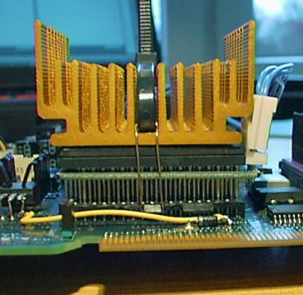
2. An external switchmode regulator
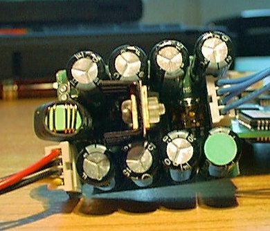
The two boards are interconnected with 4-pin plugs (blue wires) and the
regulator board is then connected to the main PSU via a standard 4-pin 3.5"
FDD power plug ("small molex"). The regulator board has 4 small SMD switches
that can be used to set the desired core voltage. The "large" golden
heatsink could be ordered separately and is not part of the base kit itself.
The interposer has a very thin and fragile pins on the bottom and has to be
carefully installed on the platform socket. You may notice that
not all pins are present on the underside of the interposer - that's
intentional, these are the pins that carry the lower core voltage. As mentioned
before that voltage is supplied by the additional voltage regulator that is
powered directly from the main PSU.
Once you have installed the interposer, CPU, regulator and CPU heatsink, the
system should come up as normal. There are jumpers on the interposer that can
be used to set the appropriate core/bus ratio (multiplier). On the 60 MHz
(unmodified) platform a 1:3 ratio will bring you to 180 MHz. For a test run I
would suggest to leave the pins open and try out the combo at the usual 90 MHz
processor speed. If that works reliably, start working your way upwards...
YARM - Yet Another Regulator Module
I've once bought this MMX interposer module together with some non-IBM
motherboard. It has a local regulator for the core voltage - yet another member
of the LT108x family, that is once again powered directly from the main PSU
via a standard 4-pin 3.5" FDD power plug. It has jumpers to set the correct
core voltage and bus/core ratio. But the whole design is a tad awkward as you
can see from the pictures below.
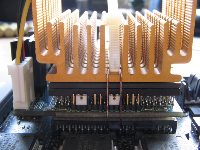
View of the DC-input and the jumpers... |
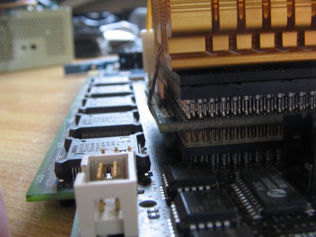
...and how the wire runs around the edge. |
| |
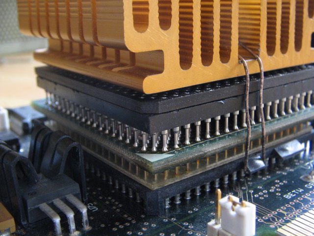
View from the MCA side upwards |
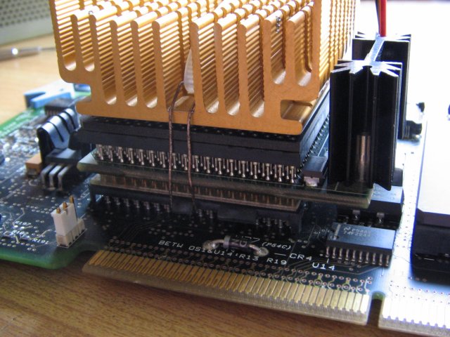
Voltage regulator with its own heatsink |
It has a couple problems. There are no catches on the CPU socket that could
be used to fix the CPU cooler. The jumpers are also placed awkwardly, right
where the heatsink clamp would normally be, which further complicates heatsink
installation.
To fix the heatsink in place I've come up with the contraption you can see
above - two pieces of wire and one zip tie. It's not ideal as the wires are
pushing against the interposer PCB and barely fit inside the socket hooks. This
also causes the heatsink to be pushed off-center. I would be a bit concerned
about reliability of this solution, if I was to run this thing for a long time
(which I don't, to be honest).
Take this as an experiment only. The complex refused to POST properly with
this combo. As always it first complained about a platform change, but then
during the refdisk load it dumped into a 0129 1500 error. I'm not 100% sure,
but I think the MMX processor I've used here was previously running in a clone
with a 3.3 V core voltage for some time... so it may be damaged. Not sure if
that's what caused the problems here, but it's possible.
Whatever, in theory it should work and you might get a similar looking
result if you manage to find one of those interposers.
|