|
3070V150.zip Reference & Diagnostic Disk for 5530-S,T/5540-T/5550-S,T,V v1.50 (DOS/V)
3070V150R.zip Reference Disk for 5530-S,T/5540-T/5550-S,T,V v1.50 (DOS/V)
3070V150D.zip Diagnostic Disk for 5530-S,T/5540-T/5550-S,T,V v1.50 (DOS/V)
3070V136.zip Reference & Diagnostic Disk for 5530/5540/5545/5550/5570 v1.36 (JDOS)
5550-S/T/V Engineering Changes
IBM PS/55 Model 5550-T Specifications/Option Price List (by Akamaki; Japanese)
IBM PS/55 Model 5550-T (5551-T09) Startup (by Akamaki; Japanese)
IBM PS/55 Model 5550-S/T/V Various Pin Assignments (by Akamaki; Japanese)
IBM PS/55 (5551-T09) SIMM memory expansion does not go well (by Akamaki; Japanese)
General Information
Japanese equivalent of PS/2 Model 70 (8570).
5550-S/T, the first desktop models in the PS/55 line, were introduced to the
market in April 1988 together with the 5570-T tower (8580 20 MHz analogous).
5550-S/T were similar to the PS/2 Model 70, but IBM Japan modified many
aspects of the original design. The most distinctive change is the number of
MCA slots. The Japanese 5550-S/T has four MCA slots, compared to 3 of the Model
70. The 4th slot was added for Japanese Display Adapter to handle Japanese
characters. For this reason the 5550 planar is a bit wider than that of the
PS/2 Model 70, and as a matter of fact, the body is slightly wider as well
(see the badge area on the photo below). The other exterior changes are fairly
minor - the type & S/N sticker has been relocated below the power switch,
and the LED/switch pictograms are slightly different as well. The base of the
chassis is made of a sheet metal instead of plastic.
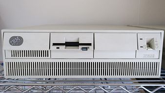
Front view of Model 5550-T (source) |

A look inside (Stage II T Planar) (source) |
5551 386 Series Lineup (-S/T/V, original HERE)
| Model |
CPU |
Memory
(std/max) |
HDD |
Video |
| 5551-S09/S19/S0A/S1A |
80386DX 16 MHz |
2/16MB |
30-60MB |
PS/55 DA |
| 5551-T09/T19/T0A/T1A/T0B/T1B |
80386DX 20 MHz |
2/16MB |
30-120MB |
PS/55 DA |
| 5551-V0A/V1A/V1B/V0B |
80386DX 25 MHz
64KB L2 cache |
4/16MB |
60-120MB |
PS/55 DA |
| 5551-V24/V28/V2B |
80386DX 25 MHz
64KB L2 cache |
4/16MB |
40-160MB |
PS/55 DA |
Stage I vs Stage II
The planar of early models S and T had some problem related to the bus
mastering feature and those planars were called Stage I. The later models that
were void of this problem were called Stage II. So there should be 4 types of
planars for S and T models and another one (or two) for 25 MHz version.
Easy way to identify Stage I and Stage II:
If the power switch lever is RED, most possibly it's Stage I.
If the power switch lever is WHITE, maybe it's Stage II.
Even if the power switch is white, systems with following serial numbers
belong to Stage I:
5551-S09 S/N before 97-19300
5551-T09 S/N before 97-44700
5551-T0A S/N before 97-58000
5551-T0B S/N before 97-93100
Most possibly switch over to Stage II from Stage I was made around May
to Jul 1990.
PS/55 System Guide - 5550 and Industrial 5500 Models
Guide
Edition |
5550 |
5502 |
| -S |
-T |
-V0 |
-V1 |
-V2 |
-S/T |
-TG |
-V2 |
-VG |
| '88-07 |
O |
O |
|
|
|
|
|
|
|
| '88-12 |
O |
O |
|
|
|
|
|
|
|
| '89-06 |
O |
O |
O |
|
|
|
|
|
|
| '90-02 |
O |
O |
O + UG |
|
|
O |
|
|
|
| '90-07 |
S1 O |
T1 O |
|
O + UG |
|
O |
|
|
|
| '90-11 |
S1 O |
T1 O |
|
O + UG |
|
O S1/T1 |
O |
O |
|
| '91-05 |
S1 O |
T1 O |
|
|
O |
O S1/T1 |
O |
|
O |
| '92-02 |
|
|
|
|
O |
O S1/T1 |
O |
|
O + UG |
O: means the model is listed in the Guide Book
+ UG: means 486DX upgrade option is also listed
Specifications
5551-S0/T0 Specifications (original HERE)
| Model name |
Model 5550-S |
Model 5550-T |
| System device name |
5551-S09 |
5551-T09 |
5551-T0A |
5551-T0B |
| Announcement date |
April 1988 |
| CPU |
i80386 16MHz |
i80386 20MHz |
| coprocessor |
Options (i80387) |
| ROM |
128KB (1Mbit) |
| Standard RAM |
2MB |
| Max RAM |
16MB |
| Display function (DA-2) |
1040x725 dots (80 columns x 25 lines of text, 12x24 dot font) |
| 1024x768 dots, 16 out of 262144 colors or 256 colors (graphic) |
| Display function (VGA) |
720x400 dots 16 colors (text 80 columns x 25 lines, 9x16 dot font) |
| 640x480 dots 16 colors (graphic) |
| FDD |
1.44MB 3.5-inch 2-mode FDD x 1 (second one can be built-in as an option) |
| HDD |
30MB |
30MB |
60MB |
120MB |
| expansion slot |
32 bit x 2, 16 bit x 2 (one of which is occupied by Display Adapter II) |
| Other I/F |
Keyboard, mouse, parallel, serial (RS-232C), display |
| Attached software |
reference diskette |
| Base price |
¥820,000 |
¥940,000 |
¥1,140,000 |
¥1,490,000 |
Reference
Ref. Ver. 1.00 to Ver.1.36 are based on JDOS.
Ref. Ver higher than 1.4x are based on DOS/V.
Ver. 1.50 covers most of of all 386 models such as 5550-S/T/V, 5570-T/V, 5540-T, 5530-T.
Video
For S, T and Vo/V1 models
As like as PS/2 8570, PS/55 5550-S/T have VGA chip on the planar. But in
order to handle true Japanese fonts, PS/55 Japanese Display Adapter II (with
AVEC connector) is equipped with earlier models of 5550-S/T (and 5570-T). VGA
port on the planar is covered with a plastic plug.
For V2 model
I'm not sure about a display adapter used for this model. V2 planar does not
have a VGA chip and it has BVE MCA slot. Then most possibly Display Adapter B
or B-2 might be equipped with V2 model.
Memory
| P/N | Capacity | Notes |
|---|
| 65X1211 | 2MB | 5550-S/T |
| 65X1212 | 4MB | 5550-T
Double-decked shape. Only one module can be used.
This module should be installed at J9( memory slot #3) |
| 23F2165 | 4MB | 5550-V0/V1. Double-decked ? |
| 79F2536 | 4MB | 5550-V, 5541-T, 5530-S/T, 5510-T |
| 79F2500 | 8MB | 5550-V, 5541-T, 5510-T |
Hard Disk Interface
Same as 8570, ESDI (roughly speaking).
Planar
There were various types of planar for 386-class 5550.
| Model |
CPU |
Planar Level |
MCA Slots |
| S |
16 MHz |
Stage I & Stage II |
4 Slots |
| T |
20 MHz |
Stage I & Stage II |
4 Slots |
| V0/V1 |
25 MHz |
|
not sure, most possibly 4 |
| V2 |
25 MHz |
|
5 slots, No VGA chip on the planar |
I've once heard that S stands for Sixteen, T stands for Twenty
and V stands for twenty-fiVe.
Stage I Planar P/N ? (S - 16 MHz), P/N 65X1377, EC 341537S (T - 20 MHz), (also used by IBM 7561/7562)
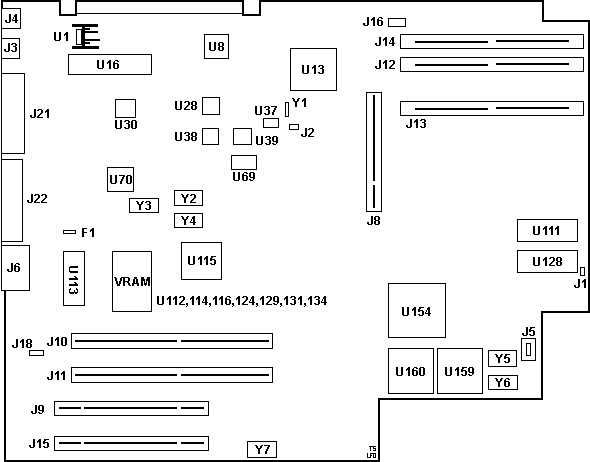
F1 1A KB/mouse fuse
J1 Unknown
J2 Pads
J3 Mouse port
J4 Keyboard port
J5 Battery/Speaker connector
J6 HDD15 video connector
J8 Floppy/Hard-drive Riser connector
J9,15 16-bit MCA slot w/ AVE
J10,11 32-bit MCA slot
J13 MEM Location 1
J12 MEM Location 2
J14 MEM Location 3
J16 4 pads only
J18 3-pin header, unknown
J21 Parallel port
J22 DB25 serial port
U1 LM340 VR
U8 NEC µPD72065L FDC
U13 72X8299 PIO
U16 P8042AH Keyboard controller
U28,38 8259A-2
|
U30 94X1265
U37 Motorola MC14069UB
U39 Motorola MC146818AFN RTC/CMOS
U69 Sanyo LC3517RM 2Kx8 SRAM (NVRAM)
U70 NS16550/AV/AFV UART
U111 65X1506 BIOS Even
U112,114,116,124,129,131,134
M5M4464AL 64Kx4 DRAM (video)
U113 Inmos IMSG171P-35 RAMDAC
U115 90X8941 VGA controller
U128 65X1507 BIOS Odd
U154 80386-20 CPU
U159 80387 Math co-pro
U160 90X8134 DMA controller
Y1 32 KHz xtal
Y2 25.175 MHz osc
Y3 1.8432 MHz osc
Y4 28.322 MHz osc
Y5 40.0000 MHz osc
Y6 32.0000 MHz osc
Y7 14.318 MHz osc
|
U111/128 2x 27512 64Kx8 BIOS EPROM (Even/Odd)
23F3012 / 23F3013 - PS/55 Model 5550, rev. ?
65X1506 / 65X1507 - IBM 7562, rev. ?
Uses the same core logic and general design as the
8570 Type 1 planar.
The Stage I S planar is probably the same except for the oscillator Y5.
Stage II Planar P/N 38F6776 (S - 16 MHz), 23F3346, 54G1612 (T - 20 MHz)
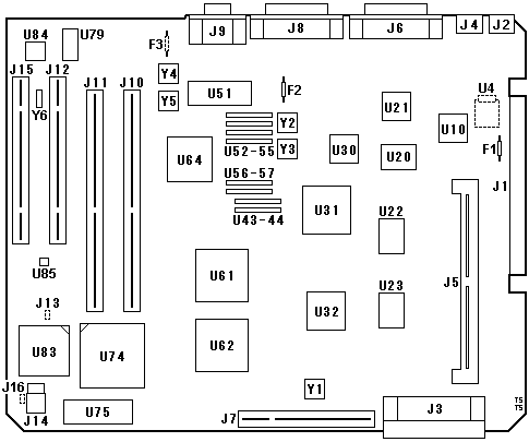
F1 2 A fuse (KB/mouse)
F2 3 A fuse (?)
F3 Pads for fuse
J1 Power connector edge card
J2 Keyboard port
J3 Memory expansion connector
J4 Mouse port
J5 72-pin SIMM socket
J6 Parallel port
J7 Floppy/Hard-drive Riser connector
J8 DB25 serial port
J9 HDD15 video connector
J10,11 32-bit MCA slot
J12,15 16-bit MCA slot w/ AVE
J13 Pads for 2-pin jumper
J14 Battery/Speaker connector
J16 Pads for 2-pin jumper
U4 Pads for LM340
U10 NEC µPD72065L FDC
U20 33F8602 FDC GA
U21 NS16550AFV UART
U22 33F5946 CPU GA
|
U23 33F5944 Memory controller GA
U30 N8042A 90X9298 Keyboard controller
U31 33F5838 I/O controller GA
U32 38F6972 EPP3 GA
U43,44,52-57 M5M446AM-12 VRAM
U51 Inmos IMSG171P-35 RAMDAC
U61 57X4111
U62 90X8134 DMA controller
U64 90X8941 VGA controller
U74 80386DX-16 (S), -20 (T) CPU
U75 38F6933 BIOS ROM
U79 LC3664NML-12 8Kx8 SRAM (NVRAM)
U83 Math co-pro socket
U84 Motorola MC146818AFN RTC/CMOS
U85 LM386 Audio op-amp (PC Speaker)
Y1 32.000 MHz (S), 40.000 MHz (T) osc (CPU)
Y2 14.318 MHz osc
Y3 24.000 MHz osc
Y4 28.322 MHz osc
Y5 25.175 MHz osc
Y6 32.768 kHz xtal (RTC)
|
U75 27C1001 128Kx8 BIOS EPROM
38F6933 - 5551-T rev. 07h / 5551-S rev. 0Ah, 04 Apr 1989
J7 is moved left, therefore the HDD/FDD
riser is different from the Stage I model (and that of the 8570).
Important: The original electrolytic capacitors are
prone to leaking! If your board is affected by this problem, you should replace
the capacitors and clean the board as soon as possible. Otherwise, the leaking
electrolyte will inevitably destroy the board! The following radial
through-hole electrolytic capacitors are used on the board:
10 µF 25 V; 20 pcs (leaked, nichicon brand)
22 µF 25 V; 5 pcs (leaked, nichicon brand)
47 µF 16 V; 1 pc (not leaked on my sample)
Polymer or tantalum capacitors can be used as an alternative.
This planar uses the same core logic as the
8570 Type 2 planar, the
Later P70 planar, and the
Type 0 processor complex.
System Memory Expansion Card For 5550-S/T Stage II Planar (P/N 38F6776)
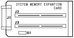
|
J1 102-pin planar connector
J2 "MEM 3" 72-pin SIMM socket (2 MB/4 MB memory slot)
J3 "MEM 2" 72-pin SIMM socket (2 MB memory slot)
U1 74LS244
|
V0/V1 (25 MHz) Planar
Outline not available.
V2 (25 MHz) Planar
As a matter of fact, I have not actually examined complete V systems ever.
I just have a V2 planar. When I draw outline of the planar, I noticed that
25 MHz V2 planar doesn't have onboard VGA. This planar has 5
MCA slots and there are solder pads for another 16-bit slot!
The bus riser slot J6 is shifted to the left compared to the S planar. It means
there should be more than three types of Bus Riser Card. Locations of bus riser
connectors are different with each other.
25 MHz V2 planar P/N 79F5325, EC C27264D
BIOS 79F2757
DL2 TQW-100
J1 Power connector edge card
J2 Mouse port
J3 CPU Daughtercard Connector
J4 Keyboard port
J5 Parallel port
J6 Bus riser (watch the location)
J7 DB25 serial port
J8 Memory slot #2
J9 Memory slot #3
J10 Pads for 16-bit MCA slot
J11 Memory slot #1
J12 16-bit MCA slot
J13,15 32-bit MCA slot
|
J14 32-bit MCA slot w/ BVE
J17 32-bit MCA slot w/ AVE
J16 Battery/Speaker connector
U14 90X8134 DMA Controller
U15 N8042 90X9298 Keyboard controller
U41 56F7502 ISERE
U46 72X8299 PIO
U66 57X4311
U73 NEC µPD72560L (typo?)
U77 NS16550 UART
Y1 32.0 MHz osc
Y2 14.3 MHz osc
Y3 40.0 MHz osc
Y4 1.8432 MHz osc
|
CPU Daughter Board
Main differences between 8570 sub board and 5550-V2 sub-board are:
- Pin orientation of 387 co-pro
- Planar-daughter board connector
Memory
From 5550-V2 system guide;
One 4MB SIMM was originally installed, expandable up to 16MB on the planar.
Option SIMM's are:
1) 4MB P/N 79F2536
2) 8MB P/N 79F2500 (only one module can be used on a planar)
Overclocking
A guy once reported that he had changed 50 MHz osc to 60 MHz and system worked
without POST error.
Riser card for HD and FDD
As written in V planar section, there are several types of bus riser cards.
I once had two types of riser card but there should be three or more.
CPU upgrade
I tested following upgrade kits on my S and T models.
- Evergreen upgrade modules with IBM486BL2 and BL3.
Cyrix and TI chips could be used on S/T models but not on V models due to 64K
L2 cache on the CPU board (I have not examined).
- Kingston MC master 486 (originally made by AOX).
I used it on T planar. MCMaster can take a 5x85 CPU but you can't use
neighboring MCA slot in order to use 5x86 CPU with a heatsink. Not a good
choice for 8570 because it has only 3 MCA slots.
- PowerBoard
In order to use a PowerBoard on S (Stage II) model, some adjustment is needed
to place the board properly.
- Need to adjust location of metal parts for screw holes to keep the planar.
Location of screw holes at left front edge is different between S and T/V.
- a Bus Riser card for FDD and ESDI hard disk for T model.
- battery and SP unit for T model.
Genuine option by IBM 80486 25 MHz Processor Upgrade Kit (P/N 57F0085) was
listed for 5551-V0x model.
5502 Industrial Computer
5502 is an industrial model number.
Industrial models are numbered as " 5500" and each model has unique number
such as 5502-S1x, -T1x and so on.
| Type |
CPU |
Memory |
HD |
FDD |
Option Slot |
|
Std |
Max |
32/16-bit |
16-bit |
| S01 |
16 MHz |
2MB |
16MB |
- |
1 |
2 |
1 |
| S11 |
16 MHz |
2MB |
16MB |
- |
1 |
2 |
1 |
| T19 |
20 MHz |
2MB |
16MB |
30MB |
1 |
2 |
1 |
| T1A |
20 MHz |
2MB |
16MB |
60MB |
1 |
2 |
1 |
| T1B |
20 MHz |
2MB |
16MB |
120MB |
1 |
2 |
1 |
| TFx |
20 MHz |
2MB |
16MB |
|
1 |
Poss same with TGx |
| TGA |
20 MHz |
2MB |
16MB |
60MB |
1 |
4 * |
1 |
| TGB |
20 MHz |
2MB |
16MB |
120MB |
1 |
4 * |
1 |
| V2A |
25 MHz |
4MB |
16MB |
80MB |
1 |
3 |
2 (half) |
| V2B |
25 MHz |
4MB |
16MB |
160MB |
1 |
3 |
2 (half) |
| VGA |
25 MHz |
4MB |
16MB |
80MB |
1 |
3 |
2 |
| VGB |
25 MHz |
4MB |
16MB |
160MB |
1 |
3 |
2 |
Number of Option Slots
System Guide describes number of Option Slots left for users except
already occupied with a Display Adapter. So basically, one slot should be added
to the number shown in a diagram.
Model S11 to T1B meet with the rule and one 16-bit AVE slot might already
be occupied with a display adapter. Then how it comes that TGA and
TGB were noted as 4 + 1? Wonder if these 2 models were
not shipped with any Display adapters and use VGA on the planar?
Next question; it seems models Vxx models DO have
activated 6th 16-bit slot shown in outline of 5550-V2 planar. 5550-V2 planar
has four 32/16-bit slots including x1 AVE and x1 BVE slot. But above diagram
shows 5500-V have three 32/16-bit slots and two 16-bit slots.
If 32/16-bit BVE slot was occupied with a Display adapter, total MCA slots
would be SIX including two 16-bit slots. Would like to see the planar.
| 
