|
rfp75a.exe P75 486 Reference Disk v1.0 (zipped image)
190-197 8573-P75 486 (8573-161 AND 8573-401)
SHS84F8525 IBM PS/2 P75 486 HMR
SHS84F7593 IBM PS/2 Model P75 486 HMS
tpvol1.pdf HMM for IBM PS/2 P70/P75 and laptops/notebooks
Patched Refdisk Files
(result of running XGAOPT on original refdisk)
P75 Errors
P75 Processor Card Mods
Failing Capacitors (14902 Error or just no video at all)
IBM PS/2 Portable Restoration (biesenhome.de)
The Fastest Portable: IBM's P75 Road Warrior (BYTE article)
P75 System Board
Indicator Port Pinout (J17)
Slot Numbers and Widths
Memory
Filling SIMM Sockets
Non-OEM Memory
64MB in a P75?
Actions On Memory Errors
Processor Card
Video Card
J1 and J2 Function
Battery Pack
Floppy Drive
Floppy Controller
2.88MB Capable?
Attempting 2.88MB
Support (Always use the stock refdisk!)
Undorking a P75
External Storage Device Connector
External Storage Device Cable Source
Remove Floppy Drive (H1 Model)
Reassemble Floppy Drive
P75 SCSI
Terminators
Remove SCSI BIOS Chips
SCSI and System BIOS Wondering
Set SCSI ID
SCSI Cable
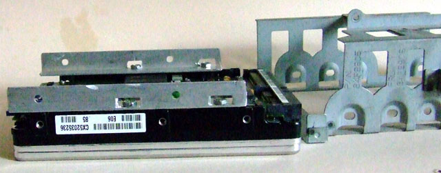
P75 Drive Carrier Screw Spacings
P75 HD Rail Dimensions
Hard Drive Mounting Rails
Hard Drive Mounted in Cage
Brightness Program
P75.EXE
Active Matrix LED Screen Prototype
Riser Swap with P70
Windows 98SE
Built-in Features ADF
Some photos sourced from biesenhome.de.
P75 Planar "IGH0445FA", FRU P/N 78F9896, P/N 78F9894 (Japanese design)
![[P]](/other/img/photo.gif "Front")
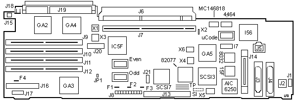
15F 15F7917
4464 Hitachi 4464S-08LL
82077 82077AA Floppy controller
8032 80C32-1 MCU (SCSI)
AIC6250 Adaptec AIC-6250EL
Even 79F3214 SCSI BIOS Even
Odd 79F3213 SCSI BIOS Odd
F1-3 Little Fuse 1.5A picofuse
F4 LF unk Amperage Fuse for floppy
GA2 64F8781 Memory Data Buffer
GA3 79F3196
GA4 79F3242
GA5 79F3202
I7 Hitachi 4464S-08LL
I56 79F3200
IC5F 90X8134(ESD) DMA Controller
J1 Keyboard
J2 Mouse
J3 Printer
J4 RS232C DB25
J5 External Floppy
J6 Display
J7 Bus riser
J8 PSU
|
J9-12 72-pin SIMM socket (SIMM1-4)
J13 SCSI internal
J14 External SCSI C60
J15 Speaker
J16 Floppy
J17 Indicator
J19 Processor
J20 MC-2
J21 HDD Power
JP1 Power On Password
MC146818 MC146818AF
SCSI3 33F6910 SCSI Data flow controller
SCSI7 33F6715 SCSI MCA iface/BM DMA controller
SI 5-pin header outline, "SCSI ID"
TP 8-pin Term Packs IR6-8
uCode P/N 79F3212
X1 20.0000 MHz osc
X2 32.768kHz? xtal
X3 14.31 MHz osc
X4 24.0000 MHz osc
X5 20000 xtal ?KHz
X6 12500 xtal ?KHz
|
Important: The original electrolytic SMD capacitors
are prone to leaking! If your board is affected by this problem, you should
replace the capacitors and clean the board as soon as possible. Otherwise, the
leaking electrolyte will inevitably destroy the board!
More information HERE.
J17 six pin header for floppy drive, power,
and hard drive LEDs
J20 MC-2 14 pin header that connects to
riser card.
J8 Wire Colors
Pin1 on left, pin 10 on right (silkscreened on board)
Blue (9), Orange (10), Red (11), R (12), R (5), Black (8), Bk (1), Bk (2), Bk
(3), White (4). Numbers in () are the corresponding power supply connector.
Indicator Port (J17) Pinout
This is the Indicator port- three LEDs are
driven off this header, Power, HD, and Floppy. Note that
the header on the system board and the display card (P/N
65X1569) are keyed, so the pins match from 1 to 1, 2 to
2, and so forth.
Pin LED
1-2 Power LED
3-4 HD LED
5-6 FDD
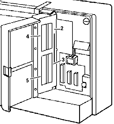
Slot Numbers and Widths
The two upper slots are 32-bit. The slot next to the rear cover has the AVE
connector. The bottom two slots are 16-bit, and they are short. FWIW, Slot 1 is
the internal SCSI controller.
|
Slot 4 (Outer Top) 32-bit MCA w/ AVE
Slot 2 (Inner Top) 32-bit MCA w/ MME
Slot 3 (Inner Bottom) 16-bit MCA
Slot 5 (Outer Bottom) 16-bit MCA
Memory expansion cards in Slot 2!
|
Memory
2 and 4 MB 70 ns parity SIMMs are supported, max 16 MB on the planar.
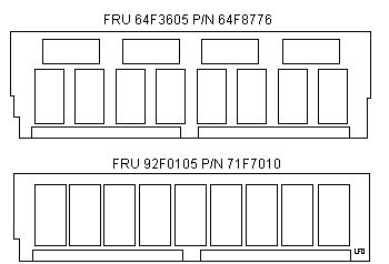
Panasonic OEM (IGH0380BA) 4MB is FRU 64F3605
P/N 64F8776
IBM 4MB FRU 92F0105 P/N 71F7010
FRU 6450128, 927200 are 4MB SIMMs from IBM, the P75 is somewhat sensitive to
positioning them, so you may have to move them around until it works.
64F3605 and 92F0105 Considerations
Memory "Manufactured by IBM" 4MB 70 ns memory, FRU P/N 64F3605 or P/N
92F0105 and 2MB 70 ns memory FRU P/N 64F3604, or P/N 92F0102 will operate in
the odd memory sockets (J9 and J11) on the 8573-P75 system. The "Manufactured
by IBM" 4MB 70 ns SIMMs has nine (9) memory modules placed vertically on one
side of the SIMM.This is due to a timing line incompatibility problem between
the system board and "Manufactured by IBM" memory. If this memory is installed
in the even number memory sockets, POST error codes or advanced diagnostics
errors such as 107, 110 with five question marks, 215, 216, or 221 can
occur.
Memory "Manufactured for IBM" has the same FRU
number but has either eight vertical and four horizontal modules on one side of
the SIMM, or it may have modules on both sides of the SIMM. Memory
"Manufactured for IBM" does not have a socket restriction and can be installed
in ODD or EVEN system memory sockets.
Update: A new 4Mb SIMM FRU P/N79F3234 is now
available for use on the 8573 P75 systems. This SIMM operates in all system
board memory locations.
Memory "Manufactured by IBM" is now used as FRU stock for the 8590 and 8595.
It is used as OPTION STOCK for the 8573 P75, 8590 and 8595. but for the
8573-P75, it is only to be installed in the ODD sockets. The 8590 and 8595 can
use either "Manufactured by IBM" or "Manufactured
for IBM" in ANY memory socket.
Thinkpad General - Model P70 And P75 Memory Checkout
Applicable to: World-Wide
Memory Checkout: Power-off computer before removing or replacing parts.
4MB memory modules installed in slots 2 or 4 must be FRU 79F3234.
Filling SIMM Sockets
When you expand the memory capacity with
2MB or 4MB SIMMs, use one of the following arrangements.
Other combinations makes the access times slower. (IBM
P75 Quick Ref, Pg. 20)
| SIMM |
OEM |
1 |
2 |
3 |
4 |
5 |
| 1 |
4MB |
4MB |
4MB |
4MB |
4MB |
4MB |
| 2 |
4MB |
4MB |
4MB |
4MB |
4MB |
4MB |
| 3 |
|
2MB |
2MB |
4MB |
4MB |
4MB |
| 4 |
|
|
2MB |
|
4MB |
2MB |
| Total |
8MB |
10MB |
12MB |
12MB |
16MB |
14MB |
Non-OEM Memory
From Louis:
What about dumping 4x4MB sticks in my P75? Yeah, get some!... What
an education! First, I dumped in 4 70 ns PS/2 SIMMs. 201/110 error. Swapped out
#3 chip, cuz it barfed at about 1200KB. Didn't do it. Swapped out the last two
4MB SIMMs with the original BIG 4MB SIMMs. Barf at 8000KB.
Well hell, I swapped the original SIMMs into MEM1 and 2, put two PS/2 SIMMs
in 3&4. Counts it, it boots. I think it's happy. Odd, does the P75 have
special mojo on the original SIMMs or what?
64MB on a P75
Ivar Amund Grimstad wrote:
I have upgraded to a total of 64MB RAM, using 12MB on the planar
and 52MB on a Kingston KTM-MC64 expansion board that fits only in the upper
32-bit slot. (Ed. I think there has to be a "memory
window" in the 16MB so you can "map" the extended memory into it. Might be able
to get 14MB on the planar with 4x4x4x2?) (Ed. Slot
2 is the MME slot)
Peter said:
>According to Peter, he's running a later Acculogic SIMMply Ram that can
utilizes four 8 Mb 72 pin parity SIMMs with only 8 Mb (two 4 Mb SIMMs installed
on the planar) for a total of 40 Mb.
That's right. The P75 is -more or less- a "Model 90 with a carrying handle".
So the 16MB memory limit does not directly apply on that machine (unlike to
Mod. 70 and 80). However: the planar memory mapper seems to be a bit odd and
needs to map in the memory on a card ("Channel Memory") into the lower 16MB to
have it addressable. That's why I had to remove memory from the
systemboard.
Interesting in this respect was the fact that I had to remove 4MB when the
Acculogic was equipped with 4 x 4MB modules and I had to remove 8MB from the
planar, when it had 4 x 8MB. Seems as if the memory granularity only adjusts to
full module values (4 or 8MB).
Action on Memory Error
The P75 allocates memory in 2MB blocks, except for the first 2MB of
system-board memory. For errors in this first block, the following occurs:
Error in First 512KB
If POST detects an error in the first 521K of system-board memory, the first
2MB block of system board memory is deactivated and the following occurs:
- If an additional 2MB block of system board memory is installed, the
addresses assigned to the deactivated block are reassigned to the second block
of sbm. This is only true for the first two 2MB blocks of system board memory.
After the first two blocks, an error code is displayed.
- If additional system board memory is not installed, no address reassignment
occurs and an error code is displayed.
- The first 512KB of memory address space cannot be assigned to adapter
memory.
Error Outside First 512KB
If POST detects a memory error in any
memory after the first 512KB of system board memory, the
2MB block of memory is not deactivated and an error code
is displayed. In this event, the customer level
diagnostics program can be run to deactivate the 2MB
block and reassign the addresses.
After the block is reassigned, the
defective block is ignored by POST during subsequent
power-ons.
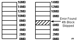
If errors occur one at a time, the system deactivates 2MB blocks of memory.
However, if two errors occur at the same time on the same SIMM, the system
programs cannot be loaded and an error message is displayed.
Processor Card "iGH0377CA", FRU P/N 64F8789, P/N 64F8775 (Japanese design)
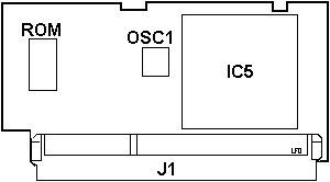
|
IC5 486DX-33 CPU (soldered!)
OSC1 66.6666 MHz osc
ROM 64F9924 (soldered!)
Plus some 74xx glue logic. Very simple board.
P75 CPU Upgrade (from Jim Shorney's site)
Jim Shorney's P75 Wizardry (documented by MAD Max)
|
Video Card "IGH0446FA", FRU P/N 78F9897, P/N 78F9895 (Japanese design)
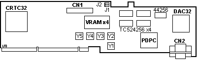
44256 Hitachi 44256S-10LL
CN1 Plasma panel
CN2 External video
CRTC32 TC110GC9AG
DAC32 37F0842
J1,2 POS ID (see HERE)
PDPC 53F8674
|
TC524256 Toshiba TC524256J-10
VRAM Toshiba TC524256AZ-10
Y1 25.175 MHz pixel clock (640x4xx)
Y2 41.539 MHz pixel clock (132-column)
Y3 28.322 MHz VGA / Text mode
Y4 44.900 MHz pixel clock (1024x768i)
Y5 40.000 MHz DMA Clock / 2
|
A lot of these are used on the XGA
adapter.
Important: The original electrolytic SMD capacitors
are prone to leaking! If your board is affected by this problem, you should
replace the capacitors and clean the board as soon as possible. Otherwise the
leaking electrolyte will inevitably destroy the board!
More information HERE.
J1 and J2 Function
Both J1 and J2 are jumpered on 2-3.
WBST:
An update on those mysterious jumpers (J1-J2) at the top of the
adapter. These apparently control the lowest 2 bits of the Adapter ID read
during planar POS setup. With them both off entirely, the Adapter ID was read
as 8DFF. With them both on 2-3 the Adapter ID was read as 8DFB (XGA). I'd guess
that the 1-2 position serves solely as a storage position.
| POSID |
8DFF |
* |
8DFB |
| J1 |
Open |
1-2 |
2-3 |
| J2 |
Open |
1-2 |
2-3 |
* Storage position
Similar functions may also apply to those on the P70 video display adapters,
possibly modifying the VGA adapter ID (EFFD) in a similar manner.
Perhaps the multi-XGA class adapter design work started with the VGA class
adapter standard?
Battery Pack PN 79F3198 (assembly),
Battery Card PN 64F8794
The P75 uses a 6V battery pack, with two Panasonic CR2477 3v 1000 mAh cells
in series soldered to a circuit board.
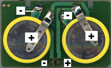
|
The battery header (J18) is a four pin header with one pin missing. The plug
on the end of the battery card cable has one position plugged.
|
J18 Pinout
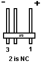
|
Battery Card plug 3 is Black, 1 is Red, 2 is NC. The battery card socket has
a plastic plug in the position of the missing pin.
|
Floppy Drive
The floppy can be used in the open or closed position. It is recommended
that it is operated in the closed position so the chance of foreign material
dropping in the drive is greatly reduced.
The floppy in my P75 is a ALPS DFP723D15C, 12 V 0.47 A, 5 V 0.16 A
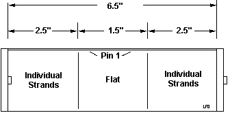
Floppy Controller
It's a 82077AA. Probably supports 2.88MB floppy drives (yea! got to love the
dust shutter), but NOT the " * " marked 2.88MB floppy drives.
2.88MB Capable BIOS?
This is from the HMM- note the reference to a "4MB Media Sensor"....
3.5-Inch Diskette Drive 38F5936
3.5-Inch Diskette Drive 38F5936 (with 4MB Sensor)
Using the 2.88MB Floppy
According to the Western Gunslinger, David Beem, the non-star 2.88 works. So
I whipped out a FRU 64F4148, Sony MP-F40W-03, and dropped it in with some
trepidation.
Installation This model has the same
layout as the original ALPS DFP723D15C. Looking from above, the drive motor is
on the left (same side as the eject button) and floppy cable is on the
right.
Note: After some thought, the cable tie holding
the floppy cable to the bracket on the PSU is most likely to assist in
positioning the floppy header during assembly. It is possible that carefully
cutting the cable tie would allow you to use a 2.88MB floppy with the 34 pin
header on either side...
Just swap the plasticized shield to the new drive (nice that the big exposed
flywheel is gone on the 2.88), and put on the rails. Because of the black dust
shutter, you can't just slap on those rails. Instead, start the rear screw
first. Now pull out on the front end of the white rail and start the front
screw. Now you can snug it down with little trouble.
Longer 2.88MB Eject Button
The 2.88 has a little longer eject button that will prevent you from closing
the floppy carrier back into the case when you have a floppy in it. BUT since
you now have a dust cover on your floppy, you might be able to live with it. If
it really bothers you, file it down (how crude).
Hacking Refdisk for 2.88MB Support
Don't try this! Do not try to cook up a hacked
refdisk using refdisks of other systems that use similar components! I did just
that and I almost trashed one of my (very few) P75s!
The problem is when you hose the POS values with the bogus refdisk, the
stock refdisk won't work! Worse, it comes up as a Non-System disk. Tim Clarke
is of the opinion that the later refdisks move the extended CMOS area, and
that's what sends the floppy to Nirvana.
Undorking a P75
I was unable to reset the CMOS with any utility that I tried, the floppy
could read the floppy, but trying to open files produced Disk not Ready
errors.
I noticed that I could boot with a PC DOS 7 boot disk, so out of hope
(desperation?) I created a PC DOS 7 bootable floppy, then dumped all the other
files (minus command.com, ibmbio.com and ibmdos.com) to the boot disk. I then
used Bob Eager's REFSTAMP on it.
The hybrid refdisk will boot to the PC DOS prompt. I then ran SC.EXE from
the command line, configured, then saved it. Sort of nice with the bootable
floppy, as soon as you hit F3 to exit, it returns you to the command line. Run
SETCLOCK.EXE to set your clock.
Shorting the MC146818AF RTC
Getting to it is half the fun. Undo the 4-40 posts from the ports, then undo
the two screws holding the left end of the MCA slot bracket, unplug the header
from the planar, unscrew the screw at the top where the braided ground comes in
from the plasma display, unscrew the screw at the bottom next to the SCSI ID
header artifact, then remove the single screw that is in the center of the "T".
Now rock the riser out of the planar. Wasn't that simple?
With power off and the battery unplugged, short pins 12 and 24 together for
15 seconds. That's the certain way to clear it, yet I am not totally convinced
it clears everything.
Pin 1 on the RTC faces left, so 12 is the rightmost pin on the bottom, and
pin 24 is the leftmost pin on the top. (Thanks to William Walsh for sending a
snippet from the newsgroups).
Stick the MCA slot bracket back on, replace all screws and posts.
Boot with the PC DOS 7/refdisk hybrid. Run SC.EXE and SETCLOCK.EXE, now the
system should (maybe, possibly) respond.
External Storage Device Connector
Shared with the P70, look HERE.
Floppy Drive Removal
From Jim Shorney (I'm an engineer, not a doctor):
OK, this is not rocket science, especially if you have an H1
floppy.
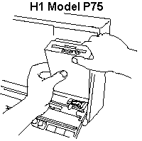
Reach in behind the display panel with your left hand. Slide your index
finger in behind the floppy housing on the left side about 3/4 of the way up.
Then slide your finger downward along the edge of the housing until it stops on
the catch. At this point, hook your finger behind the left side of the housing
and pull the side of the housing to the left, maybe 1/4" or so. Once the little
post on the floppy cover clears the catch, the floppy will flop forward.
Continue to rotate it until it is level, then pull it straight out.
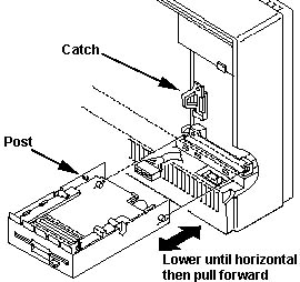
Removing Floppy from Drive Carrier, H1 Model
Unscrew both screws from the upper side of the carrier. Pull the floppy
rearward until the white plastic piece on the right side is just to the front
of the catch.
Now pull the side of the carrier away from the drive and pull the drive up
on the right side and pivoting it on the left side. Note: The floppy will NOT slide out of the carrier.
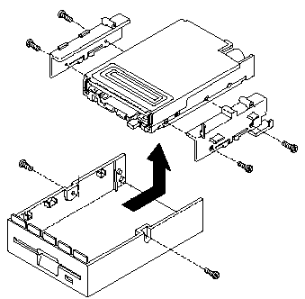
Reassembling Floppy into Drive Carrier
This had me stopped for a little bit. You have both white plastic pieces
that screw onto the front sides of the floppy. Which goes on which side?
If you look into the recess that the drive carrier fits into, you will
notice a black catch in the upper right corner. Now look at the two white
plastic pieces. Notice that one has a little "arm" sticking up? This part gets
screwed on the floppy on the same side as the eject button.
Slip the left side of the floppy into the drive carrier. Pull the right side
of the carrier out so the floppy "rail" will clear. Slide drive forward until
it stops. Install both self tapping screws.
Warning! There is a aluminum ground shield across
the bottom of the floppy drive. It is attached with four screws through the
bottom mounting holes (which are not used by the plastic "rails"). It is coated
on one side with a plastic non-conductive coating. To properly attach this
shield, the grounding strap "tab" MUST be on the same
side as the motor! A simple test- use an ohmmeter on the shield, one side
conducts, the other, not.
P75 SCSI
It resembles the newer SCSI /A with the 20 MHz / 12.5 MHz oscillators.
P75 SCSI               Tribble (new)
80C32-1 MCU            N8032AH
AIC-6250EL             AIC-6250EL
33F6910                33F6910
33F6715                33F6715
4464S-08LL             SRM2264LM12
20000 KHz xtal         20 MHz osc
12500 KHz xtal         12.5 MHz osc
15F7917                15F7917
Take a look at David Beem's SCSI
microcode levels. The latest ucode for the Tribble is 41G9974 14h/20d date
1992.
Atmel AT27C256R-15R 28 pin
SOIC [package 28R] BIOS and firmware
Package Type R - 28 Lead, 0.330" Wide, Plastic Gull Wing Small
Outline (SOIC)
SCSI BIOS PN 79F3214 (even) / PN 79F3213 (odd). SCSI microcode PN 79F3212
Ed. I had Bruce from Blue Feather Technologies burn
me some of the 92F2244 and 92F2245 SCSI BIOS in the small SOIC chips and use
them in my P75s. Up to six SCSI devices can be attached to the SCSI controller.
It supports drives up to 1.05GB.
Terminators
It uses three 8 pin, seven resistor SIPPs, 145
ohm (150 ohm will work fine). Radio Schlock has the 150
ohm #900-8143. Pin 1 is towards the SIMM sockets.
Removing SCSI BIOS Chips
I want to open my P75 and pull the SCSI BIOS chips. Might have to figure out
some way to remove them (Dremel off the carrier, then the leads?).
Dr. Jim says:
That's my boy, never use tweezers when a sledgehammer will do.
Removing the SCSI BIOS chips is trivial. The carrier is a two-piece affair.
Slide the _inner part away from the SIMM socket (you will notice a small gap at
that end of the carrier). It will make a disturbing 'snap' sound, after which
you can lift the inner portion out. The chip will lift right out into your
grubby little paws at this point. (Ed. the neat-o
SOIC socket is a Hirose DL3A-26)
SCSI and System BIOS Wondering
Peter wrote:
Today I did a bit experimenting with the 8573-401 P75 portable. I
wanted to know if and how drives over 1GB could be used in that machine.
At first I tried using a 2.1GB Quantum Fireball attached to the onboard SCSI
controller. The drive was properly recognized with 2.112MB in the setup - but
it did not show up with the proper capacity in FDISK. I tried Win95 FDISK -
which showed a size of 1.024MB (1.0GB) as estimated even with the advanced
large media support turned on.
Then I installed the short IBM PS/2 Fast SCSI-2 Adapter /A (60E9) in the
second lower 16-bit slot. The first slot contained a short 16/4 Token Ring
adapter already. While the card has no front tab it just fits between the rear
slotcover and the power supply fan without squeezing :-) A very tight fit if
you ask me. The internal SCSI cable could be detached from the planar SCSI port
and attached to the SCSI-2 card. The length is sufficient.
Now: this seems to work.
It is however not possible to configure the SCSI device(s) attached to that
controller, if you only copy the ADF to the reference disk. Most likely you
will have to use "copy an Option Disk" and get the updated SCSI.DGS, SCSIHF.DGS
and -probably- SC.EXE to the P75 reference disk. I did not do that ... so far.
Maybe later, because I only have a US-P75 reference and only a german "SCSI-2
Option Disk" - and if there is one thing how to voluntarily step in the mud
then it is mixing different language versions.
The P75 also lacks the ability to select the startup sequence - but at least
it had no problem determining that the planar SCSI only has an external CD-ROM
attached and that the 2.1GB harddisk is on the SCSI-2. FDISK got straight
through and installed a 2GB primary partition. After reboot the FORMAT C: says
"Formatting 2.012,03MB" ... which takes a while, because this particular drive
has some bad sectors, which are not hidden. Strange. But okay.
Physically the slimline Quantum drive fits into the half-height HD-cage. But
the ID-select cable has an "old raster" plug for the large jumper pins, while
the Quantum has the "mini jumpers", which are thinner and have only 1.5mm
pitch. Doesn't matter much, because once set there is no reason to have the
drive ID switched to anything else than the pre-set ID 6 (traditionally I took
ID-6 of course).
Sadly the P75 has a soldered firmware ROM on the processor card. There is no
chance to read out the ROM content *after* the system powered up - and then the
ROM is relocated to an area above 16MB and masked from access. Only the
shadow-copy remains at the addresses E000 - FFFF and is mixed with the
additional codes from the XGA and planar SCSI.
This is the same method as used on all PS/2 with 486-class processors (and
even 386 CPUs) - but these have removable ROMs that could be read and analyzed
before the POST relocates the "pure ROM code" out and only the "compatibility
part" remains. I would really like to compare e.g. a Type 2 (old) and 41G9361
Type 2 (new) code for the advanced SCSI support and try to add this to the P75
firmware ROM, which *seem* rather close to the Type 2. Technically the P75 is a
sort of Mod. 77 / Mod. 90 mix in a portable case. It has a similar memory
subsystem (single modules, unpaired) and the planar SCSI from the "Bermuda" 77,
it got the planar XGA-1 from the Mod. 90. So either of these machines -to my
opinion- could be used to filter out the additional code that enables the
planar SCSI controller to handle drives over 1GB.
On the Mod. 90 the code can be supplied with the upgrade version of the the
processor board firmware ROM - why not on the P75 ?
Anyone any idea to this ? I don't have the equipment to unsolder the SMD-ROM
undamaged or read it out. My EPROMmer takes only DIL-chips ... but that is the
least problem, because I can build / buy an adapter. The ROM itself is a
27C1001 / 27C010-version (128K x 8 bit) as far as I remember ... I have PLCC
28C010 Flash-ROMs around here ... :-)
Hey Jim - wouldn't that be another challenge to push out the P75 performance
a bit more ? The advanced SCSI support on the Mod. 77 "B" helps it to even run
8GB drives .... tried that with my old Ultimedia 77 and a Seagate Elite-9
drive, before they were installed in the 9585. No problems getting them to work
under NT 4.0.
Set SCSI ID
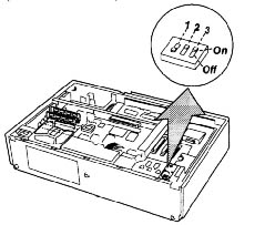
|
| ID# |
1 |
2 |
3 |
| ID6 |
Off |
On |
On |
| ID5 |
On |
Off |
On |
| ID4 |
Off |
Off |
On |
| ID3 |
On |
On |
Off |
| ID2 |
Off |
On |
Off |
| ID1 |
On |
Off |
Off |
| ID0 |
Off |
Off |
Off |
|
SCSI Cable
Note: Both SCSI connectors have the pin
holes facing UP. The length of the flat and loose is immaterial, but the OAL
should be AT LEAST 6.5". The end for the drive should use a strain relief.
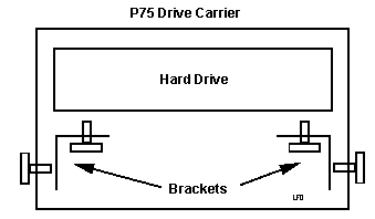
P75 Drive Carrier
My vision: Get a angle bracket, cut to length, drill mounting holes in the
top and sides.
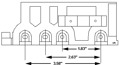
P75 HD Rail Dimensions
Dimensions are relative to the end AWAY from the SCSI connector. The
material is 1/2" aluminum angle from Ace Hardware, cut to 4.5" long. I
"flattened" the angle bracket to show the relations between the holes. Holes
are 5/32".
First hole for the rail to HD cage is .625". second hole is 3.245". Both
holes are .250" from the angle.
Note: The distance to the angle for these holes is
not critical, as long as you have clearance for the screw heads.
First hole for the HD to rail is 2.375". second hole is at 4.125". Both
holes are .125" from the angle
Note: These holes MUST be .125" away from the angle,
since the Hard Drive width can't change...
Note: The rails are
mirror images, they are NOT identical!. The dimensions
are the same, but swapped.
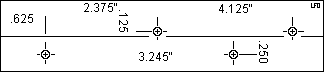
Completed HD Mounting Rails
I finally took matters into my own hands... Took 4.5" lengths of 1/2"
aluminum angle and drilled some 5/32" holes. Note the mounting hole for the
left end (farthest from the SCSI connector) is the same distance as the old
0661 HD. Oddly, the spacing between that hole and the first screw for the
new(er) HD is 1.75", and the second HD mounting hole is 1.75" past that...
Odd...
The HD mounting holes are .125" from the edge of the angle, and interfere
with installing the screw, so I used a keyway cutter to mill away a slot to
give the screw head clearance. The holes to mount the rails are 5/32 for now,
but I'm thinking of switching to a mild steel angle because the extruded
aluminum is soft. I could have tapped it for 10/32, but I'm afraid that it
would be too easy to strip the threads from aluminum.
P75 HD Cage with Drive Rails
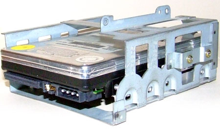
Here's a shot with the drive on the rails. I used 3/8ths inch 8x32 nylon
machine screws and nuts from Ace Hardware. The nylon screws were a close fit in
the 5/32" holes, almost like a barbed fastener... You might just stick with
5/32 and nylon screws for a quick assembly. Note: The
aluminum angle used may make "shavings" when threaded for use with steel
screws. Consider threading for 8x32 and use nylon screws...I wonder if a thread
forming tap would work.
Using aluminum is OK, but be careful of threading.. Use the same diameter
drill for all holes if you can. Use a 1/2" diameter by 3/16" wide keyway
cutter. A .750" dia cutter leaves too much flash. If you use an ER-20 collet
chuck, get a 3/8" shaft keyway cutter so it fits...
Brightness Program
To install Brightness program, run BRTINST.COM from the refdisk. This
installs BRT.COM.
To have emphasized text brighter than standard text, type "BRT" and press
Enter. To have standard text brighter than emphasized text, type "BRT /H" and
press Enter.
The P75 has XGA-1 with 1MB VRAM.
The internal display however supports only the 640 x 480 mode and turns off
if any of the higher modes is used. This will explain why you can get a picture
on the external screen but not on the plasma.
You will have to stay at the low-res mode here, since the display is from
the principle only a "generic VGA screen" (same as on the P70 BTW).
P75.EXE
While the system is running, this utility allows you to switch from the IBM
external display attached to the XGA2 Adapter and the plasma display or the IBM
external display attached to the XGA external port. To do this, just type
P75 at a dos prompt and the XGA2 Adapter with the monitor connected will be
disabled and video will output to the plasma display or the display hooked to
the XGA port.
Type "P75/u" at dos prompt (undo) option to return to the monitor connected
to the XGA2 Adapter.
Active Matrix LED Screen Prototype
Source: "IBM Rolls Out 22-Pound, 486 'Luggable' PC" by Ed Scannell,
InfoWorld 19 Nov 1990, Pages 1 and 141
(Google Books)
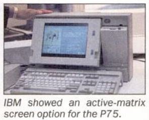
As part of the announcement, the company last week demonstrated a flat-panel
color display it jointly developed with Toshiba. However, IBM officials
declined to say if it would be available for the P75. The color display is
scheduled to be delivered in the first half of 1991, IBM officials said.
Reversing Course:
IBM’s Strategic Recovery in the Flat Panel Display Industry
The big move came in 1986 when IBM entered into a two-year joint research
alliance with Japanese manufacturer Toshiba focused explicitly on full-color,
active matrix (AM) LCD TFTs. IBM initially considered other partners such as
GE, Sharp, Matsushita, and Hitachi but settled on Toshiba in part because
“they were probably hungrier than others” and in part because, at that
point, Toshiba had built the largest prototype.
The relationship initially focused on proving that the smaller (2”-3”)
LCD televisions could be effectively scaled up to larger sizes, and then moved
to the creation of a 14” full color prototype computer display. In 1988 the
two firms signed a joint venture agreement to create Display Technologies Inc.
(DTI) and build a manufacturing facility in Himeji City in Japan next to an
existing Toshiba monochrome LCD plant. By 1991, DTI had created the monitor for
the P75 portable and in 1992 for the first IBM ThinkPad. In 1992, DTI produced
around 500,000 TFT panels for use by IBM and Toshiba, as well as for sale to
other companies.
Riser Swap with P70
Ever thought of using a P75 riser on a P70? Well, it won't work. The riser
may physically fit, but the P75 has a 14-pin header from the planar to the
riser card. Of course, the P70 lacks it entirely. Probably the extra control
lines?
Win98SE on P75
Peter says:
Today I have tested my trusty old "PortaPotty" 8573-401 (P75
Luggable) with Win98SE. My configuration: unmodified 486DX-33, 8MB (2 x 4) on
the planar, 32MB (4 x 8) on the Acculogic Simmply RAM, Madge 16/4 TR (TROPIC
chipset), Maxtor MXT540S at SCSI-ID6, external CD-ROM II (caddy loaded) in
3510-AV0 enclosure.
Win98SE install took about 3 hours ... I went away in between for lunch and
missed to "press any key". The system hung at one point prior to the first
reboot after the files had been copied from the CD and before you are asked to
enter the 4 x 5 ident characters. I switched the machine off and powered it
back on. Caused no major problem except waiting for the 40 Megs RAM to count
up.
Result (after that long time): "Your system is optimal configured". No
16-bit mode, full access to the CD-ROM etc. pp. ... but it is rather slow.
Guess I'll have to send in the processor board to Doctor Jim for some
supercharging ... :-)
P75 System ADF
0E0FFh AdapterName "Built In Features"
Serial Port
Serial 1 through Serial 8, or disabled.
<SERIAL_1
03f8-03ff int 4>, 2 (02f8-02ff int 3), 3
(3220-3227 int 3), 4 (3228-322f int 3), 5 (4220-4227 int
3), 6 (4228-422f int 3), 7 (5220-5227 int 3), 5 (228
-522f int 3), Disabled
Parallel Port
Parallel 1 through
Parallel 4 or disabled.
<PARALLEL_1
03bc-03bf 1278-127f int 7>, PARALLEL_2
0378-037f int 7, PARALLEL_3 0278-027f int 7, PARALLEL_4
1378-137f int 7, Disabled
Parallel Port Arbitration Level
Arbitration levels 0 through 7.
<Disabled> places parallel port in compatibility mode.
<Level 6>,
5, 4, 3, 1, 0, Disabled, Level 7
Preempt Enable/Disable
System board CPU can preempt continuous
data transfers by other devices on the MCA bus.
<Enable>,
Disable
Video I/O Address
I/O address range for Display Controller
Registers and location of video coprocessor registers.
<Instance
6: 2160h - 216Fh>, Instance 1: 2110h -
211Fh, Instance 2: 2120h - 212Fh, Instance 3: 2130h -
213Fh, Instance 4: 2140h - 214Fh, Instance 5: 2150h -
215Fh
Video ROM Address Space
Memory address range used by system
video ROM.
<C0000
- C1FFF>, C200-C3FF, C400-C5FF, C600-C7FF,
C800-C9FF, CA00-CBFF, CC00-CDFF, CE00-CFFF, D000-D1FF,
D200-D3FF, D400-D5FF, D600-D7FF, D800-D9FF, DA00-DBFF,
DC0-DDFF, DE00-DFFF
Video Arbitration Level
The video
sub-system can use any available arbitration from level
8 through 14.
<Arbitration
level 13>, 12, 11, 10, 9, 8, 14
Video Fairness
Whether or
not video sub-system coprocessor follows the fairness
algorithm for bus usage.
<Fairness
On>, Fairness Off
Auto-Dim Time
Auto-Dim
function automatically turns plasma display off after
specified period if no input from the keyboard or
auxiliary device is received. Auto-Dim Time can be from
1 to 120 minutes.
<10
Minutes>, 20 Minutes, 30 Minutes, 60
Minutes, 120 Minutes, 1 Minute,5 Minutes
Auto-Dim Reset
There are two ways to turn on the display
again:
1. Pressing SHIFT
2. Clicking the mouse.
If the mouse
picks up vibration on a desk which turns on the display
again, change Auto-Dim Reset from <Keyboard and Aux.
Device> to <Keyboard Only>.
<Keyboard and Aux. Device>,
Keyboard Only
Color to Gray Mapping
Some applications that are
developed for color displays can be used on monochrome
displays. For such applications, reset Color-to-Gray
Mapping to <Green Signal Only>. Setting <RGB
Mixed Signals> may result in an unpredictable display image.
<RGB Mixed Signals>,
Green Signal Only
Turned-on Display
Primary turns
on only one display that is considered to be the primary display.
No external display -
Plasma is primary display. Only VGA is supported.
External display - External is
primary display. VGA or XGA supported on external port
Plasma and External
turns on both plasma and external display. Only VGA mode
is supported.
<Primary>,
Plasma and External
|