|
Introduction
Installing and Removing Cache
Module Types
Compatible Cache Sources
Module IDs and Compatibility
Cache Error 0129090x
Module Pinout
Documentation
Introduction
The 128-pin modules discussed here are an all-in-one Level 2 cache solution
designed specifically for 486-class systems. They integrate not only the cache
SRAM chips but also the cache controller logic. Modules with different write
policies (Write-Through and/or Write-Back) and cache sizes (128 and 256 KB) are
available. While the form factor may look similar to the COAST ("Cache On A
STick") modules used in many later Pentium systems, the two use very different
interface and architecture (and needless to say, are totally incompatible).
This is essentially the 485Turbocache Module
in a different formfactor and with some additional signals to support
Write-Back cache policy and module type identification.
The 128-pin L2 cache modules are used by the following IBM and Reply
planars:
Note: Even though all these 128-pin modules share
the same physical and electrical interface, only some of them are actually
supported by the PS/2 systems. There are several aspects that potentially limit
the compatibility. Namely - the processor support logic, system firmware
(POST/BIOS), and also the type of the installed CPU.
There has been a number of efforts to deduce the proper choice of WT/WB
with certain processors. But if you search the newsgroup, some boards work one
way, then move the CPU and cache to another board, and it bombs. Whatever works
for you...
Installing and Removing Cache
|
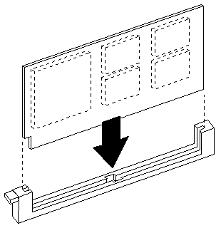
Installing Cache Module
Note the notch on the bottom of the module on the corner. Now, look at the
cache socket. There's a white plastic latch on one end of the slot. Insert the
cache module so that the notch is towards the latch.
Removing Cache Module
If you want to remove the cache module, pull up on the white latch (it's a
captive part!) until the notched corner of the cache module is pushed out of
the socket. The module is released now and can be removed by hand.
|
Note: While there is enough space in the 9585 K/N
unit to unlatch the module with just your fingers, the Lacuna-based machines
are much more cramped so it can be difficult to reach the tab and pull it. To
make the job easier, just sneak a small screwdriver, drill bit, or what have
you under the latch and then pull on both ends of it to release the latch.
Module Types
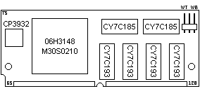
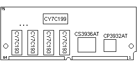
Cypress 128 KB WT/WB L2 Cache FRU P/N 06H3306, P/N 06H3306
![[P]](/other/img/photo.gif "Front") |
|
OKI M30S0210-033, 06H3148 Cache Controller
CY7C185 8Kx8 CMOS SRAM
CY7C193 32Kx8 Synchronous SRAM
CP3932AT PLL?
Shipped with some Lacuna-based models 76/77 i/s.
WB mode compatible only with the 33 MHz Lacuna.
WB mode not compatible with 85 K/N (clock timing issues?).
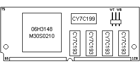
Cypress 256 KB WT/WB L2 Cache FRU P/N 06H3307, P/N 82G6938
OKI M30S0210-033, 06H3148 Cache Controller
CY7C193 32Kx8 Synchronous SRAM
CY7C199 32Kx8 Static RAM
CS3936AT
CP3932AT PLL?
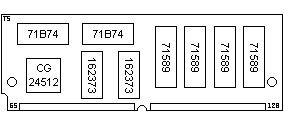
IDT 7MP6104 128 KB WT L2 Cache (datasheet)
(photos from pchistory.lv)
Fairchild CG24512 Cache Controller
IDT74FCT162373 16-bit Latch
IDT71B74 8Kx8 Cache-TAG SRAM
IDT71589 32Kx9 Cache SRAM, Burst Mode 486
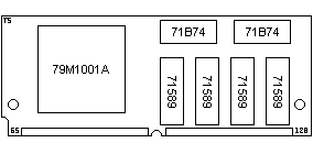
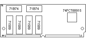
IDT 7MP6150 256 KB WB L2 Cache
IDT 79M1001A Cache Controller/State Machine
71B74 8Kx8 BiCMOS Cache Tag
71589 32Kx9 CMOS, Burst Mode 486
74FCT88915 PLL Clock Generator
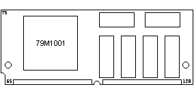
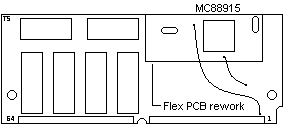
IDT 7MP6108 256 KB WB LC Cache
IDT 79M1001A Cache Controller/State Machine
MC88915FN70 Low Skew PLL driver
SRAM chips not marked, probably the same as on the 7MP6150 module (or equivalent).
Shipped with the Model 85 N.
Compatible with the 33 MHz Lacuna-based systems.
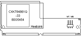
Sony 128 KB L2 WT/WB Cache FRU P/N 39H0865, P/N 39H0864 or 85G4865
CXK784861Q-33 (AQ-33) 80G5454 "Sony Cache-1C" - Single-chip Cache Subsystem
This "Super Cache" module is shipped with the Japanese PC720.
Compatible with the Lacuna-based systems (33 MHz both WT/WB, 25 MHz WT only).
Compatible Cache Sources
From Aron Eisenpress (edited):
The Lacuna cache modules physically fit the ValuePoint 2 (VP2)
systems - namely the 6382/S, 6384/D, and 6387/T.
Not the 6384's with 30-pin
SIMMs, which are so-called ValuePoint 1 (VP1) systems,
nor the Pentium 60 models,
nor the Si or "Performance" models.
Here are the IDT modules I know about:
- 7MP6104: 128 KB WT for Lacuna
- 7MP6107: 128 KB WB for VP2; works fine there.
(photo)
- 7MP6108: 256 KB WB for VP2; works fine
in WT but not reliable in WB mode. I didn't have a Lacuna to test this in then.
- 7MP6150: 256 KB WB for VP2; seems to work well.
- 7MP6155: 256 KB, I think it's WT. This
does not work properly in the VP2 with a CPU faster than a 486DX33, and when
I tried it in the 76s it worked but I got a message saying that the copy of
the FAT in memory was bad... so I don't think it works properly there either!
Maybe the chips are too slow or something. We got these as add-ons at the time
we bought a bunch of VP2 DX33's, so I presume they're supposed to work in them.
- 7MP6188: 128 KB WT. Seems to work in
the 76s and also in the VP2.
- ? There's another one which is 256 KB
WB and worked fine in my 6382/S but I can't seem to find a record of what the
number was and I no longer have that system.
Module IDs and Compatibility
The table below is based on information from the
IDT datasheets,
Technical Reference documents for the
Model 76/77 i/s
and
Server 85
systems, and on observations made by analyzing the system firmware (POST/BIOS).
Please note that there may be some additional conditions affecting what
modules are actually compatible with your system - including the timing specs
of the module, the type of installed CPU (the table below assumes the original
CPU to be present), etc.
| ID Bits | Module
Type | Compatibility |
|---|
| 2 | 1 | 0 | Lacuna
25 MHz | Lacuna
33 MHz | 85 K/N |
|---|
| 1 | 1 | 1 | 128 KB, WT | Yes | Yes | No [7] |
| 1 | 1 | 0 | 256 KB, WT | Yes | Yes | No [6] |
| 1 | 0 | 1 | 512 KB, WT | No [A] | No [A] | No [5] |
| 1 | 0 | 0 | 1 MB, WT | No [8] | No [8] | No [4] |
|
| 0 | 1 | 1 | 128 KB, WB | No [6] | Yes | Yes |
| 0 | 1 | 0 | 256 KB, WB | No [4] | Yes | Yes |
| 0 | 0 | 1 | 512 KB, WB | No [2] | No [2] | No [1] |
| 0 | 0 | 0 | 1 MB, WB | No [0] | No [0] | No [0] |
Cache Error 0129090x
If a particular module isn't supported by the system, it will report error
0129090x "Cache memory kit is not supported" where x is ID of the installed
module. The 85 K/N systems report decimal representation of the 3-bit cache
module ID as one would expect. The Lacuna-based machines make things a little
bit more confusing by reporting the hexadecimal value of the ID multiplied by 2
(this is because the POST code considers even the presence detect bit when
calculating the value). See the table above for the
reported IDs [in square brackets].
For example:
- 85 K/N with 128 KB WT/WB module set to WT gives error 01290907
- 25 MHz Lacuna with 128 KB WT/WB module set to WB gives error 01290906
In some cases, the system fails to POST at all, freezes or gets stuck in an
infinite restart loop.
Module Pinout
| Pin | Signal | | Pin | Signal |
|---|
| 65 | GND | 1 | GND |
| 66 | RESET | 2 | CLK |
| 67 | Vcc | 3 | Vcc |
| 68 | INV* | 4 | -CBOFF* |
| 69 | M/-IO | 5 | D/-C |
| 70 | -FLUSH | 6 | -BLAST |
| 71 | -EADS | 7 | -BOFF |
| 72 | GND | 8 | GND |
| 73 | -ADS | 9 | W/-R |
| 74 | -BE0 | 10 | -BE1 |
| 75 | -BE2 | 11 | -BE3 |
| 76 | PWT* | 12 | -CS |
| 77 | -CRDY | 13 | -CKEN |
| 78 | GND | 14 | GND |
| 79 | -CBRDY | 15 | PULL_UP or -BRDYO* |
| 80 | -SKEN | 16 | -START |
| 81 | WP | 17 | -CHITM* |
| 82 | -PRSN | 18 | -HITM* |
| 83 | WB/-WT* | 19 | -LOCK* |
| 84 | ID2* | 20 | PCD* |
| 85 | A2 | 21 | A3 |
| 86 | Vcc | 22 | Vcc |
| 87 | A4 | 23 | A5 |
| 88 | A6 | 24 | A7 |
| 89 | A8 | 25 | A9 |
| 90 | A10 | 26 | A11 |
| 91 | A12 | 27 | A13 |
| 92 | A14 | 28 | A15 |
| 93 | A16 | 29 | A17 |
| 94 | GND | 30 | GND |
| 95 | A18 | 31 | A19 |
| 96 | A20 | 32 | A21 |
| 97 | A22 | 33 | A23 |
| 98 | A24 | 34 | A25 |
| 99 | A26 | 35 | A27 |
| 100 | A28 | 36 | A29 |
| 101 | A30 | 37 | A31 |
| 102 | GND | 38 | GND |
| 103 | D0 | 39 | D1 |
| 104 | D2 | 40 | D3 |
| 105 | D4 | 41 | D5 |
| 106 | Vcc | 42 | Vcc |
| 107 | D6 | 43 | D7 |
| 108 | GND | 44 | GND |
| 109 | DP0 | 45 | DP1 |
| 110 | D8 | 46 | D9 |
| 111 | D10 | 47 | D11 |
| 112 | D12 | 48 | D13 |
| 113 | GND | 49 | GND |
| 114 | D14 | 50 | D15 |
| 115 | D16 | 51 | D17 |
| 116 | D18 | 52 | D19 |
| 117 | D20 | 53 | D21 |
| 118 | GND | 54 | GND |
| 119 | D22 | 55 | D23 |
| 120 | DP2 | 56 | DP3 |
| 121 | D24 | 57 | D25 |
| 122 | D26 | 58 | D27 |
| 123 | GND | 59 | GND |
| 124 | D28 | 60 | D29 |
| 125 | D30 | 61 | D31 |
| 126 | Vcc | 62 | Vcc |
| 127 | ID1 | 63 | ID0 |
| 128 | GND | 64 | GND |
* signal only present on WB modules
Additional signals compared to the 485Turbocache:
INV, PWT, -CBOFF, D/-C, -LOCK, PCD, WB/-WT, ID0-3, -CHITM, -HITM
Missing signals compared to the 485Turbocache:
-WPSTRP
For description of the individual signals see
IDT Specialized Memories and Modules (page 1040 phys.).
Documentation
Relevant data books:
IDT High-Performance Static RAMs (1992)
IDT Specialized Memories and Modules (1994)
IDT7MP6104/5 - 128KB/256KB Secondary Cache Module for i486 (page 1027 phys.)
IDT7MP6118/9 - 128KB/256KB Secondary Cache Module for i486 (page 1040 phys.)
IDT Specialized Memories and Modules (1993)
CYM7485 - 128K Write-Through Secondary Cache Module (page 1423 phys.)
| 