|
Table of Contents
[-0-] Version History, Disclaimer & Legal Info
[-1-] Precautions and Warnings before you start
[-2-] Introduction to the Type 4 "Y" Pentium 90 Platform
[-3-] The importance of cooling certain components
[-4-] Modification A) Using a Pentium Overdrive 180 / 200
[-5-] Modification B) Hardwiring the BF0 / BF1 Pins for different Bus / Core ratios
[-6-] Modification C) Changing the Base Clock from 60 to 66 MHz
[-7-] Modification D) Using a Pentium MMX 233 MHz with an Interposer
[-8-] Problems, Workarounds and other stuff
Content by Peter H. Wendt (original HERE). Edited by Major Tom.
Problems, Workarounds and other stuff
Fixing the Regulator Misery - German Approach
Those of you who don't like to compromise and want
to prevent problems rather than fix them later on, may consider this
very different approach I've tried recently.
Sitting in "the lab" one morning at a very early hour, being quite
uninspired and bored, I've started digging in my boxes full of "unsorted
stuff". During that a bag fell into my hand containing no less than 4
switch-mode voltage regulator modules (VRMs) for the bigger IBM
Netfinity machines (5600 or 6000R). They are designed for a single
+12 V DC input and have a programmable 1.3 - 3.5 V DC output @ up to 16 A,
intended for the Pentium III or Xeon processors.
Remembering the problem I had with the overheating
LT1084CT 3.3V regulator on the P90 platform, I thought it may be a good
idea to try substituting the linear regulator with the switching VRM.
20 minutes later my 9595-B06 RAID box ran with a P133 CPU (I had no faster
spare at that time) on the P90 platform, and with the Netfinity switching
VRM. The module gets merely hand-warm. The bigger one of the two coils heats
up a little - but that's it. No comparison to the "space heater" LT1084
with its flimsy heatsink.
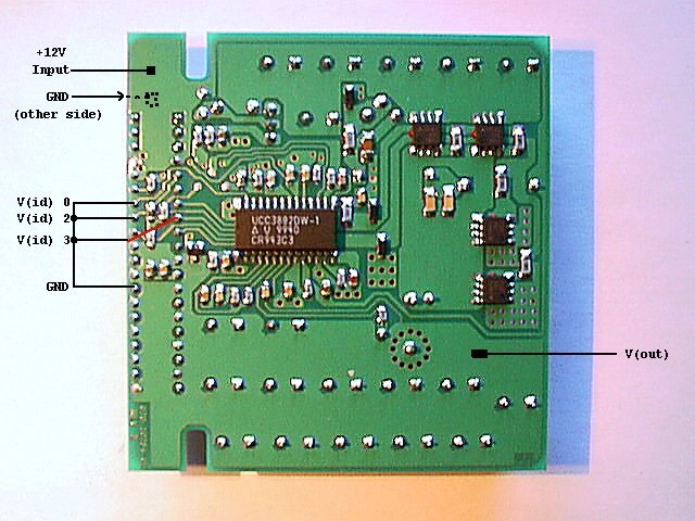
+-----+ +---------.
| | | .
| A B| | . A = outer, lower row - B = inner, upper row
| +--+ .
| .
| o o 01 . N.C. N.C.
| o o . N.C. N.C.
| o o . N.C. N.C.
| # # . +12V input +12V input
| # o . +12V input Reserved
| o o . Ishare Output Enable
| # o . V-ID 0 V-ID 1
| # # . V-ID 2 V-ID 3
| o o . V-ID 4 Power Good
| o o . V(out) GND
| o o . GND V(out)
| o o . V(out) GND
| o o . GND V(out)
| o o . V(out) GND
| o o . GND V(out)
| o o . V(out) GND
| o o . GND V(out)
| o o . V(out) GND
| o o . GND V(out)
| o o 20 . V(out) GND
| .
| +--+ .
| | | .
| | | .
+-----+ +---------.
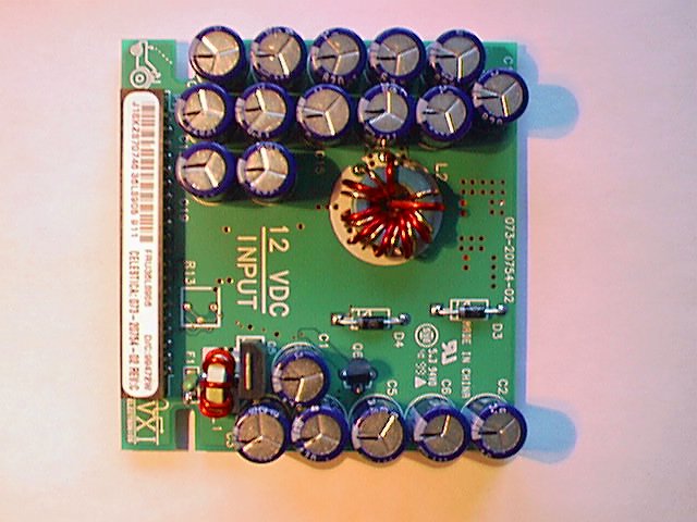
Voltage Regulator FRU 36L8906
12V-only, step-down programmable
Underside View
(Pinout according to Intel Specs V8.1)
|
| VID4 |
VID3 |
VID2 |
VID1 |
VID0 |
V(out) |
| 1 |
1 |
1 |
1 |
1 |
Disabled |
| 1 |
1 |
1 |
1 |
0 |
2.1 |
| 1 |
1 |
1 |
0 |
1 |
2.2 |
| 1 |
1 |
1 |
0 |
0 |
2.3 |
| 1 |
1 |
0 |
1 |
1 |
2.4 |
| 1 |
1 |
0 |
1 |
0 |
2.5 |
| 1 |
1 |
0 |
0 |
1 |
2.6 |
| 1 |
1 |
0 |
0 |
0 |
2.7 |
| 1 |
0 |
1 |
1 |
1 |
2.8 |
| 1 |
0 |
1 |
1 |
0 |
2.9 |
| 1 |
0 |
1 |
0 |
1 |
3.0 |
| 1 |
0 |
1 |
0 |
0 |
3.1 |
| 1 |
0 |
0 |
1 |
1 |
3.2 |
| 1 |
0 |
0 |
1 |
0 |
3.3 |
| 1 |
0 |
0 |
0 |
1 |
3.4 |
| 1 |
0 |
0 |
0 |
0 |
3.5 |
"0" = tied to
GND, "1" = left open or tied to input voltage
|
Voltage Identification Code (partial)
As you can see above, the pinout is pretty simple.
The table shows ID codes for the different output voltages.
Three Steps To Heaven
Step 1: Removing the LT1084 and its heatsink
Start by unsoldering the heatsink holder tab.
It may need a bit more heat and a little pulling force to come
free. The heatsink tab isn't electrically connected to anything on the board
- so it's mot fatal if you manage to rip the pad or pull the via out off
the board. But be careful anyway...
Then add some flux (and maybe some fresh solder) and unsolder the 3 LT1084
terminals from the board. You might try unsoldering all 3 at the same time,
and remove the regulator by gently pulling and wiggling it sideways.
Remove solder from at least the middle hole (with a solder sucker if you have
one), and then clean the entire area around the regulator from any leftover
solder or flux residue.
Step 2: Preparing the Switchmode Voltage Regulator
On my regulator most of the upper copper surface is ground, and
most of the bottom surface is either the +12 V input or the output.
I've decided not to bother with any connectors and go with just a direct
wire connections. So, I've scratched a 2 by 6 mm spot clear of the solder
mask of the GND plane, and of the +12 V input plane, and soldered two thick
wires directly to the board. On the other end of these wires is a standard
"molex" plug that fits directly to the 9595 power supply. Later I've replaced
it with a male-female extension (as for these silly processor fans) - that way
I still have all 3 PSU connectors available to me for other purposes.
Some thin "patch wires" connect the pins V(id)0, V(id)2 and V(id)3 with
the nearest GND pin (pick any - there are plenty of them).
Bench-testing with a bare 95 power supply gives a straight 3.34 V
output on the V(out) plane/pins. The voltage did not drop significantly when
being loaded with 6 A (a couple of parallel 4.7 ohm / 25 W resistors).
Heat-emission: almost non-existent. One the converter coil L2 gets a bit warm.
 |
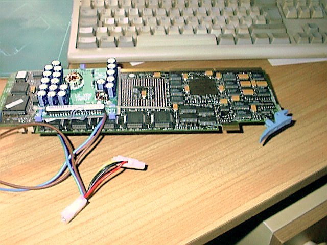
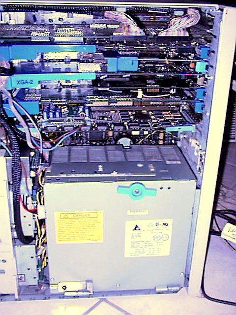
Step 3: Installing on the P90 Platform
Now, there is no provision for fixing the regulator anywhere.
The simplest method was just to strap it onto the upper side of the
processor complex. It's relatively flat, there is enough room (given you don't
have a long MCA board installed in the bottom-most slot #8) and the way down
to the power supply as well as to the solder pads of the removed LT1084 is
relatively short.
The output voltage is fed with a short, thick piece of isolated silver
wire (~ 1 mm diameter) from the regulator down to the middle pin of the
removed LT regulator. In addition I've cut a piece of thin cardboard to act
as an insulator sheet between the regulator and the processor board.
There are some larger holes in the P90 PCB: one close to the
Op Panel SDL connector and one to the right from the 82497 cache
controller. A thin zip ties will fit through these...
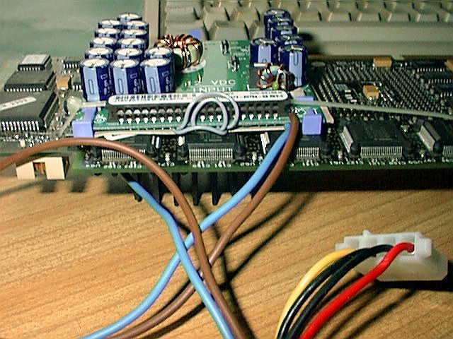
The result will probably look similar to that shown below:
Warning! With a voltage module of this caliber,
any mistake in wiring or part selection/installation, may cause massive damage!
The little LT1084 regulator would collapse at around 5 A, but a
baby like this can pump 16 A (or more!) into the circuit and it's being fed
directly from the power supply - unit that can deliver 35 - 45 A at 12 V.
That will blow the CPU out of the socket if it isn't oriented correctly.
And will - most likely - cause massive damage to the PCB itself as well.
|