|
@8EE6.ADF SGI Micro-Channel IRISVISION Adapter
Roger Brown's Site (local copy)
SGI IrisVision add-in 3D accelerator for PC (1990) (by Jiří Zima)
The Very Unofficial IrisVison Home Page (by Roger Brown, archived)
IrisGL Application Programming Interface (same as below, but HTML, archived)
Graphics Library Programming Guide, Volume I
Graphics Library Programming Guide, Volume II
Drivers & Software
Documentation
Product Description
IrisVision General Components
IrisVision Block Diagrams
MGE2 Base Card
MRV2 Raster Video Card
MZB1 24-bit Z-Buffer Option
MEV2 24-bit Frame Buffer Option
ISA vs MCA MEV2
Video Timing Parameters
ADF Sections
RS/6000
Known as "sabine" or .devices.mca.8ee6 in the RS/6000 world. Two variants:
"FC (2780) 8-Bit 3D Color Graphics Processor (Type 1-3)"
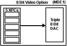
w/ 8-bit MDE1 / 71F1117 daughter card (description)
"FC (2781) 24-Bit 3D Color Graphics Processor (Type 1-3)"
w/ 24-bit MEV2 / 71F1114 daughter card (description)
Drivers & Software
IrisVision software, 24-bit color demos, and IrisView DXF file viewer
Autodesk ADI Combined Display/Rendering driver
Windows 3.x ver 2.30 display driver disk image
IrisVision GL Software Developer's Kit v 2.10 disk image
Note to PS/2 Micro Channel Users: The
Windows display driver (above) are for the ISA IRISVISION card, only.
Unfortunately, it seems when Pellucid developed this driver, they did not
include support for the MCA version of the board set.
IV1WinSrc.zip
IrisVision Win 3.1 driver source - Thanks to Resman (Glory be unto him!)
Documentation
IRISVISION Owner's Guide
IRISVIEW User Guide
ADI Driver User's Guide
(all from Lorenzo Mollicone)
IrisVision Technical Reference
Table of Contents
CHAPTER 1 Overview
CHAPTER 2 Hardware Configurations
CHAPTER 3 Host Interface Subsystem
CHAPTER 4 Geometry Subsystem
CHAPTER 5 Token Definitions
CHAPTER 6 Raster Subsystem
CHAPTER 7 Display Subsystem
(about 700 pages, from Roger Brown)
Product Description
Ed. The IrisVision hardware
lacks hardware support for certain "high end"
IrisGL features, such as texture mapping, alpha blending, accumulation, and
stencil buffers!
The following text is stolen from
Roger Brown's The
Very Unofficial IrisVison Home Page.
Hardware
The IrisVision hardware is nearly identical to the graphics sub-system in
the SGI Personal Iris workstation introduced in 1988. The hardware supports a
5th generation geometry processing pipeline, the GE5, an 8 or 24 bit per pixel
frame buffer, and a 24-bit per pixel z-buffer for hidden surface removal. The
card set implements in hardware, the entire IrisGL graphics Application
Programming Interface (API).
Notable differences from the Personal Iris graphics are:
- Uses 256K VRAM instead of 64K VRAM for reduced size
- Has a 3 color cursor instead of 1 color for increased visibility
- Has VGA pass-through capability for PC compatibility
The card has a rich set of video and rendering modes consistent with the
Personal Iris.
Origins of the IrisVision
The product came to life originally as an OEM graphics board set based upon
the VME bus in the Personal IRIS. Later, IBM approached SGI to develop a Micro
Channel Architecture (MCA) version of the card for use in their newly
introduced RS/6000 Unix workstation. IBM licensed the MCA card design as well
as the IrisGL graphics library from SGI.
In the process of testing the product, it was discovered that an IBM PS/2
Model 70 personal computer running OS/2 could be used to run diagnostics and
test programs on the card much easier than using the RS/6000. So a minimal
device driver was written for the card and soon IBM was shipping product.
(Ed. Roger Brown can't find the "minimal OS/2
drivers" and he works for SGI.)
At some point, the light went off in someone's head; "Why don't we sell this
board set for use in PCs?". IrisVision was born. Initially, the MCA card was
re-designed to offer some features critical for the PC market, including
standard 15-pin VGA-style video output and a 15-pin VGA passthrough input
connector. The IBM genlock connector was moved to the top of the card, and
stereo display signals were also brought out to the VGA passthrough connector.
The card occupied 1 32-bit MCA slot and an adjacent 16/32 bit slot. One or two
daughter boards provided framebuffer and z-buffer memory.
Work then began on the design of an Industry Standard Architecture (ISA or
AT-bus) version of the card. It would occupy 2 16-bit ISA slots and use the
identical daughter cards as the MCA (and IBM) versions of the board set.
Software
The IrisGL API is implemented in a C-language library developed with the
Metaware High-C 32-bit C compiler and the PharLap 32-bit DOS-Extender. It was
designed to run in a full screen DOS environment. At the time, M/S Windows did
not offer a 32-bit programming environment, so the PharLap DOS-Extender
technology was the most sophisticated solution available. It features full
32-bit virtual addressing (2 GB application space), virtual memory support, and
seamless integration of real and protected mode programs. The MetaWare High-C
compiler is ANSI compatible and is just the ticket for compiling Unix source
code to run under DOS-Extender on the IrisVision card.
IrisVision General Components
MGE2
Base Card (Card has both GE and HI)
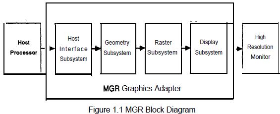
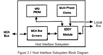
The Host Interface subsystem interfaces to the host
processor via the Micro Channel Architecture (MCA) bus. It
provides all of the necessary data and control signals
required by the MCA bus. It also interfaces to the other
three subsystems over a local bus which is compatible with
the SGI private bus. The Host Interface Subsystem provides
the programmable Option Select (POS) registers which are
used to configure the MCA bus interface aspects of the
adapter.
MGE2
Geometry Engine Subsystem
The Geometry subsystem contains the Geometry Engine which
is used to perform the geometric transformations and
lighting calculations on the graphics data. It also
performs the clipping and high level rendering
calculations before sending the data to the Raster
subsystem. The Geometry Engine performs high speed
floating point calculations under the control of the
onboard microcode.
MGE2
Host System Interface
The host system issues commands to the Geometry Engine by
sending command tokens and data parameters down a FIFO.
The Geometry Engine reads the FIFO and performs the
desired functions. The Geometry Subsystem also contains
hardware which controls the addressing of the hardware
components in the Raster and Display Subsystems.
MRV2
Raster Video (both Raster and Display
Subsystems)
The Raster subsystem receives instructions and other
data parameters from the Geometry
Subsystem and does the low level rendering of the data
into the image frame buffer bitplanes. It also handles
the 2 buffer depth comparisons and updates if the
optional Z buffer card is installed. The pixel values
for each of the 1.3 million pixels on the 1280 by 1024
high resolution monitor are stored in the video random
access memory (VRAM) frame buffer for display on the
monitor at a selected refresh rate.
The Raster Subsystem provides the necessary data and
control signals to manage the frame buffer bitplanes as
well as the Window ID bitplanes and the Auxiliary
bitplanes. The Window ID bitplanes are used to control
the display format for up to sixteen different on screen
windows. The Auxiliary bitplanes are used for drawing
pop-up menus, overlays and underlays. The Raster
Subsystem also contains two hardware cursor chips.
MRV2
Raster Video (both Raster and Display Subsystems)
The Display Subsystem performs the
necessary operations to convert the frame buffer image
data into analog RGB signals which are sent to the high
resolution RGB monitor. The Display Subsystem uses the
Window ID bitplane data to determine the format of the
pixel data stored in the frame buffer. The frame buffer
pixel data can be either a color index value or an RGB
value. The frame buffer bitplanes can also be subdivided
into two buffers for flicker free motion of on screen
objects.
The Display Subsystem performs the necessary
operations to access the frame buffer as a single buffer
or as a double buffer. The Digital-to-Analog Converters
(DACs) are used to convert the digital RGB data into
analog RGB data which output to the monitor. The Display
Subsystem also provides the necessary timing signals to
allow four different types of monitors to be connected
to the adapter.
IrisVision Block Diagrams
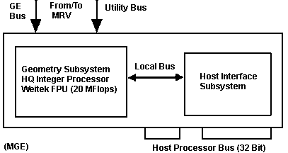
MGE2 Base Card FRU P/N 42F6842

P2 Geometry Engine Bus
P3 Utility Bus
U15 SGI L1A5205 53F3269
U17 40.000 MHz
U25 SGI L1A3578 HQ1
|
U47-51 IDT 7201
U62 Weitek XL-3132 100-GCD
U64 MGE 7951 (VPD)
U67 SGI L1A4252 GRF1
U26-29,36,38,40,42,44 IDT 7164
|
XL-3132 Floating Point Processor
Datasheet
This is the Micro Channel Geometry Engine. It is based upon
the HQ integer processor from SGI (rated at 10 MIPS) and the
Weitek XL-3132 floating point processor (rated at 20
MFLOPS). The geometry engine provides the host
interface, handles DMA operations, and handles all the
matrix operations, lighting and coordinate
transformations.
GRFl Gate Array
Provides two finish flags and corrects some
other minor design flaws in the HQl chip.
EDDY Module (U15?)
The Eddy module is the main component of the Host
Interface Subsystem. It is responsible for providing
the MCA bus interface to the host system. It is also
responsible for providing a Local bus interface to the
Geometry Subsystem which is compatible with the SGI
private bus. The Eddy module is a Bus Master DMA /
Memory Slave device for the Micro Channel
Architecture.The Eddy module will support a variety of
modes of data transfer on the MCA bus, which include:
- Setup Cycles
- 32-bit Memory Slave Cycles
- 32-bit Normal Bus Master Cycles
- 32-bit Bus Master Data Streaming Cycles
The Eddy module only responds to
32-bit Masters when operating as a Memory Slave
device. All data transfers to the local bus are 32-bit
transfers. The Bus Master DMA feature of the Eddy
module will always perform a 32-bit transfer and
therefore should always be programmed to transfer data
to or from system memory (i.e. 32-bit Slave Memory).
The following paragraphs describe the address decoding
performed by the Eddy Module.
The Eddy module provides a bus
translation from the MCA bus to the Local Bus,
the Programmable Option Select (POS) registers and the
Control / Status registers
Address Decode Section:
responsible for control
of read and write operations to POS
registers, memory mapped I/O registers and memory
mapped control / status registers.
Programmable Option Select (POS)
registers contain
information to identify and configure the adapter,s
eliminating the need for hardware jumpers. There are
eight directly addressable 8 bit POS registers, as
shown in Figure 3.3. Four sub-data registers are
accessible through the use of a sub-addressing
facility. One of the POS registers indicates channel
check status information which is only valid is after
an error has caused the Eddy module to Channel Check
the host system.
Note:
I want to illustrate the options. POS and Bit numbers
omitted at random.
- MGR adapter ID
- Interrupt Request (IRQ) Level
- Card enable/disable bit
- Byte Order Selection bit
- Wait State Selection bit
- DMA block transfer size and DMA Bus Master enable/disable bit
- Data Streaming Mode enable/disable bit
- Error checking enable/disable bits .
- Memory address
- Arbitration Level
- Fairness enable/disable bit
- Channel Check Status
- VPD subaddress registers
Note: Channel Check
Status / Sub-Address Register (POS 6) has two functions
which are controlled by the status bit (bit 6) of the
POS 5 register. If the status bit is 1, this register is
defined as a sub-address register. If the status bit is
a 0, this register contains status information about the
pending Channel Check.
Remember the RS/6000 9-K 10/100 bit Ethernet? It has
that PCI to MCA bridge chip (ASIC by AMD) and a bog
standard PCI Fast Ethernet controller. Speculation is
that XPOS are used to access the PCI Ethernet chip, but
we would need to dump the ODT for it in order to find
out...
Control / Status Section
contains the seven
32-bit registers as shown in Figure 3.4. Some of the
32 bit registers are accessible as multiple 8 or 16
bit registers. The byte ordering of the host machine
will affect the address required for accessing the
registers when accessing 8 or 16 bit portions of the
32 bit registers. These registers are defined in the
registers section of this chapter.
The Eddy module contains two DMA
channels. Each channel will arbitrate for the Micro
Channel on the same arbitration level. These channels
will operate in a serial manner so that a transfer on
one channel will complete before a transfer on the
other channel can begin. If an error occurs during a
DMA transfer, that transfer will be terminated. The
other channel will not be able to begin a transfer
until the one that was terminated is allowed to
complete.
VPD PROM
Only the identification and location of the
adapter can be determined from the POS registers. The
vital Product Data (VPD) PROM provides additional
information about the adapter. It is accessible
through the use of the POS Subaddressing Extension
which is described later in the section on the POS
registers.
The MGR adapter has a VPD PROM on each of the five
cards which are used to form the base and enhanced
configurations. Each VPD PROM is 256 bytes and
contains the following data:
- VPD Header
- VPD ASCII characters
- VPD total length
- CRC on data within the VPD PROM
VPD data fields:
- Card Description
- Engineering Change Level
- Part Number
- Manufacturer
- Field Replaceable Unit Number
- Next VPD Address
- Loadable Microcode Level
- Serial Number - unique for each card
Note:
Thank SGI, each VPD chip is socketed into individual
pin sockets!
Multi-Phase Clocks Section
Provides the necessary clock signals to the Eddy
module. It also provides the various 10 MHz clocks to
the Local Bus with the necessary phase relationships.
MCA Bus Drivers
Provide the necessary drive levels as
required by the Micro Channel specification. The Eddy
module has the ability to control the direction and
tri-state nature of these devices.
Geometry Subsystem
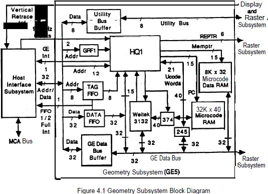
The HQ1 chip controls address
decoding for host and acts as a microcode sequencer.
The Weitek 3132 chip performs floating point
calculations and is controlled by HQ1. The microcode
RAM holds the microcode, while the microcode data RAM
holds constants, data variables and data buffers.
These four components form the Geometry Engine 5 (GE5)
which performs the geometry calculations, lighting
calculations and various other functions.
HQl Chip
The Head Quarters (HQl) chip is a proprietary Silicon
Graphics design and is the main control element in the
Geometry Subsystem. The HQl is responsible for
controlling the geometry engine and various data
transfers among MGR hardware components. The HO1 chip
has six functional units as shown in Figure 4.2.
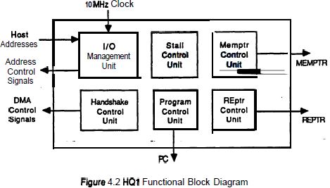
I/O Management Unit
Responsible for providing address decoding and bus control
for hardware accesses by the Host Interface Subsystem and
Geometry Engine.
Handshake Control Unit
Used to provide necessary hardware handshake
signals between Host Interface Subsystem, Raster
Engine (RE) in the Raster Subsystem, microcode code and
data RAM and XMAP2 or XPCl chips in Display Subsystem. It
stalls GE5 when appropriate and passes other handshakes
through for accesses such as host to XMAP or host to RE.
The handshake control unit allows two types of transfers
between the Host Interface Subsystem and the other MGR
Subsystems. These two types of transfers are single word
transfers and DMA transfers.
Stall Control Unit
Responsible for stalling the GE5 when a condition
arises that requires it to be stalled. The full stall
keeps the I/O Management unit in its current state and
also keeps the PC, MEMPTR and REPTR from changing. The
clock to the Weitek 3132 is fully suppressed and the
entire GE5 is literally stalled.
PC Control Unit
Acts as a microcode sequencer for the GE5.
The control unit controls microcode instruction execution
sequencing through up to 32K words of microcode. The PC
control unit allows branching and conditional jumps. It
uses a 15 bit wide PC to access microcode code RAM.
Microcode instructions are read from the address pointed
to by the PC and are executed by the HQ1 and the Weitek
3132 chip.
MEMPTR Control Unit
Used as a data pointer for accessing words in
microcode data RAM. MEMPTR is 14 bits wide allowing a
maximum microcode data RAM size of 16K words. The MGR has
only 8K words of microcode data RAM and each microcode
data RAM word is 32 bits wide. The MEMPTR is loaded from
microcode instructions to perform microcode data RAM
accesses by the microcode.
REPTR Control Unit
Used as an address pointer to RE registers.
It is used by GE5 microcode to load RE registers. REPTR is
not accessible by host which means that host cannot
directly access RE registers. A microcode token GE_LOADRE
allows the host to load RE registers with an assist from
microcode. The host generally does not access RE register
directly and exceptions will be discussed later.
GE Data Bus Buffer
This is a 32 bit buffer which allows data to
be passed between the GE5 bus and the host interface.
Single word transfers use this data path to transfer data
between the host and the microcode code RAM, the microcode
data RAM and the HQ1 PC register. DMA transfers between
the host and the microcode data RAM or between the host
and the Raster Engine also use this data path.
Utility Bus Buffer
This is an eight bit transceiver which allows
data to pass between the host bus and the utility bus.
Only the low byte of the local bus are passed on to the
utility bus. The address decoding and control signal
generation are handled by the HQ1.
MRV2 Raster Video Card FRU P/N 71F1151

J1 W3 video port
J2 GENLOCK port
P2 Geometry Engine Bus
P3 Utility Bus
P4 RGB Video
P5 Video Bus
P6 Utility Bus
P7 Pixel Bus
P8 Z Buffer Utility Bus
U1 M1244 - 30MHz osc
U2 M1244 - 24.545452 MHz osc
|
U10 L1A4996 RE 2.1 C
U23-27 TC524258AJ-10
U28-32 TC524258AJ-10
U33-37 TC524258AJ-10
U38 Bt431KJP
U39 Bt431KJP
U47 Bt438KJP
U42 XC2018-70
U43 27C256
U46 111.518MHz osc
U60 MRV 1149 (VPD)
|
Bt431KJP Monolithic CMOS 64x64 Pixel Cursor Generator
Bt438KJP 250 MHz Clock Generator Chip for CMOS RAMDACs
30MHz osc - 15MHz for PAL and SECAM
24.54542MHz osc - 12.27MHz for RS170 30 Hz (NTSC)
111.518MHz osc - 1280x1024 at 60 Hz (NI) and 30 Hz
(Int)
MC10H115P Quad Line Receiver
MC10H135P Dual J-K Master-Slave Flip-Flop
MC10H121P 4-Wide OR-AND/OR-AND Gate
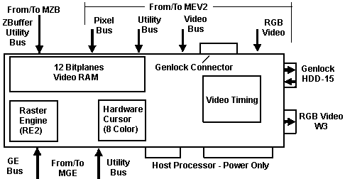
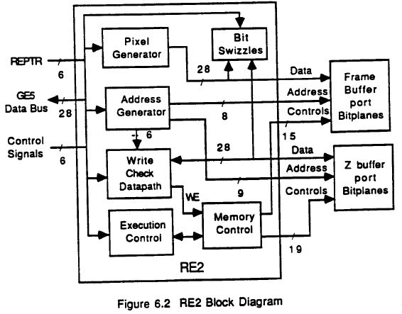
This is the Micro Channel Raster Video Engine. It is based upon the RE 2.1
raster engine chip from SGI. The raster engine provides all the per-fragment
and -pixel operations. It also contains the raster scanning hardware and video
signal generation circuitry. It only obtains power and ground from the bus, no
other bus signals are used. In addition to the two ribbon cables from the
Geometry Engine, a third connection services the Genlock features of the Raster
Engine.
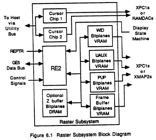
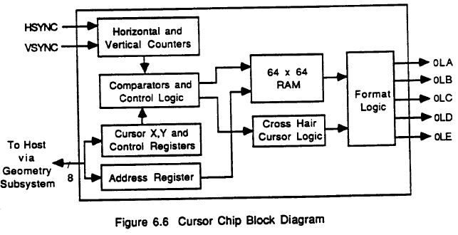
The Display State Machine (DSM) is built out of a XILINX 2018 programmable
logic array, an 8K by 8-bit RAM, a Bt438 clock generator chip and other
miscellaneous clock control circuitry. The 8K PROM contains the Xilinx logic
configuration data and the four different monitor timing tables. On system
reset the logic configuration is loaded into the Xilinx chip and the monitor
timing tables are copied to the 2K RAM for faster access. The operation of the
DSM is controlled by various bits in the display registers.
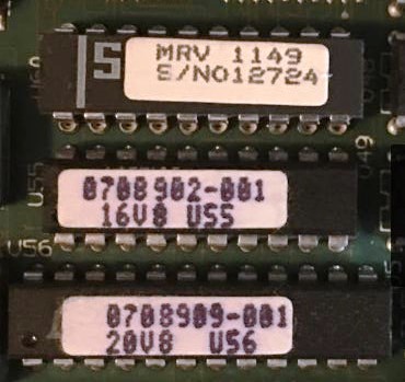
I cannot prove any of this... Right below U60 is two PLDs, a 16V8 and a
20V8.
Other than you can burn these to make anything you want, I've got
nothing.
On the card edge connector, are the VGA passthrough connector and the HiRes
video output connector. The Raster Video card contains the basic 8-bitplanes of
framebuffer memory as well as 2 bitplanes of overlay framebuffer and 2 bits of
window ID bitplanes, for a total of 12 bpp.
This card features an RGB video output connector (large w/plug-style
connectors) and a genlock input/output connector (15-pin DSUB).
The MZB1 plugs onto the back (circuitboard side) of this card (use the short
screws). The MEV2 plugs on to the front side (component side) of the card (use
long screws).
MZB1 24-bit Z-Buffer Option FRU P/N 42F6889
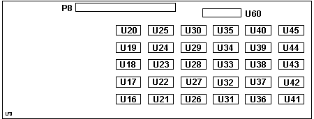
P8 Z-Buffer Utility Bus
U16-45 TMS44C256DJ-10 or TC514256AJ-10
U60 MZB 7923 (VPD)
This is the optional 24-bit hardware Z-buffer card. The function of the
Z-buffer is to perform hidden surface removal via a depth test mechanism. In
the traditional application, each pixel's "Z" coordinate value is tested
against the value already present in that location in the Z-buffer. If it is
smaller (i.e. closer to the eye) the pixel is updated with the current value
and the Z-buffer is updated. By controlling the Z-buffer operation, a number of
other useful operations can performed.
For non-3D applications, the Z-buffer can be used as an off-screen memory
buffer for saving the contents of the normal framebuffer. As no host to adapter
memory transfer takes place, this operation is very fast. The Z-buffer is
implemented in dynamic RAM (DRAM) and consists of 3.75 MB of DRAM.
MEV2 24-bit Frame Buffer Option FRU P/N 71F1114
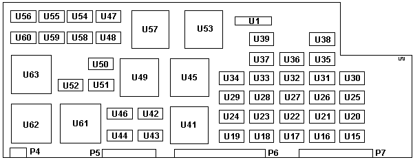
P4 RGB Video
P5 Video Bus
P6 Utility Bus
P7 Pixel Bus
U1 MEV 1112 (VPD)
|
U15-39 Toshiba TC524258AJ-10
U42-44,46-48,50-52,54-56,58-60 IDT 7164
U61-63 Brooktree Bt457KPJ125
U41,45,49,53,57 SGI XMAP2 L1A5081
|
Bt457KPJ125 125 MHz
Monolithic CMOS 256 Color Palette RAMDAC
This card supplies additional bitplanes of memory to bring the system to 24
bits per pixel of normal framebuffer in addition to 2 additional overlay/popup
bitplanes and 2 additional window ID planes, for a total of 32-bits per pixel.
A fully configured frame buffer has a total of 1280x1024*(32/8) or 5MB of video
RAM (VRAM) implemented in 256Kx8 ICs.
You'll notice that the VRAM is laid out in a 5xN array of chips. Each chip
supplies 256 horizontal pixels (1280/5 = 256). However, to achieve greater
performance, the raster engine chip is designed to write up to 5 pixels at a
time, so the five VRAM chips are interleaved; the first supplies pixels 1, 6,
11, etc. the second 2, 7, 12, etc. and so on.
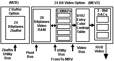
The MEV2 card is a daughter board which attaches to the MRV2 card. It has a
VPD PROM and provides an additional 20 bitplanes of VRAM which are part of the
Raster subsystem.
It also contains the five XMAPP2 chips, the 8K color map chip and the three
DAC chips which are part of the Display subsystem and are described in the
chapter on the Display subsystem. The card has the Utility bus, Video bus,
Pixel bus and RGB connections described above for the MRV2 card.
ISA vs MCA MEV2
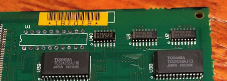
MEV2 ISA
MEV2 MCA
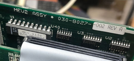
Of course, the internal traces may be different, but the PCB layouts sure
look the same, except the ISA version lacks U1 [not needed for ISA].
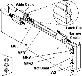
Connector cable (wide) 53F3271 80 pin .025 pitch HPDB
Connector cable (narrow) 53F3272 40 pin .025 pitch HPDB
Removing Connector Cable
Squeeze the metal clips on the ends of the connectors and pull
connector off header.
Plugging Connector Cables Back On
Squeeze the metal clips so that the loose ends of the clip enter
the catch on the header.
The following block diagram is derived from the
IrisVision Block Diagram on The
Very Unofficial IrisVison Home Page.
Video Timing Parameters
| Video Resolution |
| Parameter |
High |
Stereo |
Medium |
NTSC |
PAL |
| Pixel Clock (MHz) |
107.3 |
107.3 |
64.00 |
12.27 |
15.00 |
| Horizontal Freq (kHz) |
63.9 |
63.9 |
48.78 |
15.73 |
15.63 |
| Frame Rate (Hz) |
60.0 |
120.0 |
60.00 |
29.97 |
25.00 |
| Field Rate (Hz) |
60.0 |
120.0 |
60.00 |
59.94 |
50.00 |
| Horizontal |
| Visible Pixels |
1280 |
1280 |
1024 |
640 |
768 |
| Line Period (us) |
15.70 |
|
20.63 |
63.56 |
64.00 |
| Blanking (us) |
3.73 |
|
4.69 |
11.00 |
12.00 |
| Front Porch (us) |
0.28 |
|
1.10 |
1.63 |
1.67 |
| Sync Width (us) |
1.12 |
|
1.25 |
4.89 |
4.67 |
| Back Porch (us) |
2.34 |
|
2.34 |
4.48 |
5.67 |
| Vertical |
| Visible Lines |
1024 |
492 |
768 |
480 |
576 |
| Front Porch (ms) |
0.047 |
|
0.062 |
0.191 |
0.160 |
| Sync Width (ms) |
0.047 |
|
0.062 |
0.191 |
0.160 |
| Back Porch (ms) |
0.450 |
|
0.804 |
0.890 |
1.280 |
Original TXT version archived HERE. Local copy HERE.
ADF Sections AdapterId 8EE6h "SGI Micro-Channel IRISVISION Adapter"
Interrupt Level
Determines the interrupt level used by IRISVISION Adapter.
<" Level 2 " >,
3, 4, 5, 6, 9, 10, 11, 12
Memory Mapped I/O Address Range
Determines the range of Memory Mapped I/O addresses used by the
IRISVISION Adapter. The addresses in this range cannot be used by any other
installed device.
<"0C0000 to 0C7FFF">,
0C8000 to 0CFFFF, 0D0000 to 0D7FFF, 0D8000 to 0DFFFF
Arbitration Level
Determines the bus arbitration level used.
<" Arb Level 1 ">,
0, 2, 3, 4, 5, 6, 7, 8, 9, 10, 11, 12, 13, 14
|